Device Modelling
To enable successful device fabrication modelling is an essential tool. Researchers across our Device Modelling activities deliver both fundamental and commercially-driven research across a number of fields, including Flexible Electronic Systems, Statistical Variability, Quantum Transport, and Circuit Simulation.
Staff
| Dr Fikru Adamu-Lema | Dr Vihar Georgiev |
| Professor Asen Asenov | Dr Hadi Heidari |
| Professor Scott Roy |
Quick Links
Flexible Electronics Device Modelling
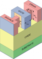
Current organic-based flexible electronics are insufficient to meet the high performance requirements and device stability needed in many applications, including displays. In this regard, ultra-thin flexible chips are a promising alternative as they enable compact and bendable electronics. Si chips are traditionally built on wafers whose thickness are about 500µm. However, these wafers are intrinsically brittle and therefore crack easily when we try to bend them. Bendable Si chips overcome this challenge by reducing the thickness of wafers to about 20μm.
The bending of chips on the flexible substrates induces stresses in the integrated electronics, which leads to changes in the I-V characteristics. Standard device models available today are insufficient to capture this piezoresistive behaviour and hence the circuit design becomes challenging. In the BEST group, we are addressing this issue by analysing the effect of uniaxial stress on the MOS devices on ultra-thin chips and developing new models based on these observations. By taking into account the bendability induced changes (e.g. in mobility, threshold voltage etc.), we are advancing the state of the art in device modelling to enable designing of circuits over flexible substrates and also advance the commercial circuit simulation tools.
Device Modelling Group
Modelling and simulation provides deep insight into the operation of modern semiconductor devices and circuits, and dramatically reduces the development costs and time-to-market. The Device Modelling Group develops state-of-the-art simulation tools which exploit finite element 2D and 3D methods, a realistic band particle Monte Carlo approach, quantum transport techniques, and the power of parallel computing. It supports and leads device technology and design programmes in the department, partner universities and industry.
Further information can be found on the group webpages: http://web.eng.gla.ac.uk/groups/devmod/
Research topics
Statistical Variability
Monte Carlo Transport
Quantum Transport
Oxide Reliability
Compact Models
Circuit Simulation
Process Simulation
Molecular Electronics
Statistical Variability
Dr Fikru Adamu-Lema, Professor Asen Asenov, Professor Scott Roy
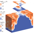
With the continuous down-scaling of semiconductor devices including MOSFETs into nanometer scale, the intrinsic parameter fluctuation introduced by discreteness of charges and granularity of matter such as random discrete dopants (RDD), line edge roughness (LER), polysilicon gate granularity (PSG) and metal gate granularity (MGG) is a significant concern in terms of device scaling and circuit yield. Those variability sources have been identified and comprehensively studied in conventional bulk transistors. In addition, the spatially random interface trapped charges (ITC) in progressive N/PBTI degradation in the background of inherent time-zero statistical variability add the statistical aspect of reliability, increasing the variability with stress time. Novel MOSFET architectures such as FD-SOI and FinFET aiming to improve short-channel effects and control statistical variability are being introduced at 22nm technology and the study of statistical variability in these architectures is critically important in evaluating further scaling and integration.
For many years members of the group have developed the world-leading statistical variability and reliability ‘atomistic’ simulator Garand. Garand has been licenced for commercial use to Gold Standard Simulations, Ltd.
Monte Carlo Transport
Professor Asen Asenov, Professor Scott Roy
The Glasgow 3D Monte Carlo simulator is a generalised device simulator developed in concert with, and now available as a module in, Garand - the Glasgow 'atomistic' device simulator. It has been designed specifically for the investigation of intrinsic statistical device variability where variation in carrier transport, in addition to electrostatic modulation, is an important consideration. It is complimentary to the drift-diffusion module of Garand, working in the same simulation domain and with the same sources of statistical variability.
The general design of the simulator allows the simulation of electron and hole transport within Silicon, Germanium and III-V materials in combination with all relevant sources of statistical variability in a variety of device structures from conventional bulk through to IFQW and FinFET. Scattering is captured through a combination of traditional bulk scattering rate models and directly via the quantum corrected potential that is most accurate for treating position dependent scattering from random dopants and interface roughness that leads to transport variation between microscopically unique devices.
Quantum Transport
Professor Asen Asenov, Dr Vihar Georgiev, Professor Scott Roy
Our Quantum Transport Simulations are based on self-consistent solution of Poisson's equation and non-equilibrium Green’s function (NEGF) approach. NEGF formalism is a generalization of the Landauer’s formalism to treat many body systems at room temperature in context of one particle. The electrostatic potential and the electron density, which serve as an initial condition for the Poisson-NEGF cycle, are obtained from a density gradient of Drift-Diffusion equations. The Hamiltonian used in the discretization of the NEGF equations is an effective-mass Hamiltonian that folds the full crystal interaction into the electron effective masses. We can perform calculations in ballistic and scattering regime where in the latter case sources of incoherent scattering such as phonon interaction, are currently included in NEGF module. The Poisson-NEGF cycle is iterated until density and current converges. We developed two methods based on either fully-3D or coupled mode space approach self-consistent methodology to solve electron transport equations. The NEGF module is included in the 'atomistic' simulator Garand.
Oxide Reliability
Dr Fikru Adamu-Lema, Professor Asen Asenov, Professor Scott Roy
Device reliability and aging in nano-scale MOSFETs is a major concern within the semiconductor industry. The device performance degradation stems from both as-manufactured oxide defects and wear-out defects generated during the operational lifetime. The former lead to initial statistical variations of electrical characteristics and the latter induce time dependent variability in the device reliability. This variability is exacerbated by the atomistic nature of matter and charges. Therefore in nanoscale devices, variability and reliability cannot be seen as separate concepts: reliability must be reinterpreted as a time dependent form of variability.
To capture the statistical nature of device reliability, we are developing a comprehensive framework that accommodates the physical kinetics of trapping and detrapping mechanisms in presence of various sources of variability like Random Dopants Fluctuations, Line Edge Roughness and Metal Grain Granularity. This simulation tools allow modelling of a large range of degradation related processes like Random Telegraphic Noise (RTN), Bias Temperature Instabilities (BTI) and Trap Assisted Tunneling (TAT), fashioning them into the common framework of the charge trapping phenomenology.
Fully integrated in the 3D atomistic device simulator, Garand, our computational scheme addresses reliability concerns for various device architectures like SOI, FinFET and BULK MOSFETs and can assess statistical based reliability predictions using large device ensembles.
Compact Models
Professor Asen Asenov, Professor Scott Roy
Compact Models are the bridge between technology, circuit simulations and design. Based on the Gold Standard Simulations compact model extraction toolkit Mystic, we are developing robust physics based nominal and statistical compact modelling strategies for Bulk, SOI and FinFET technologies.
Based on the parameter sensitivity analysis, a two-stage direct statistical compact modelling extraction procedure is developed to transfer device variability information into compact models without any pre-assumption of parameter distribution and correlation. The parameter statistical distribution information obtained from direct extraction will serve as the input for statistical parameter generation engines, which have been integrated into the Gold Standard Simulations statistical circuit simulation tool RandomSpice. Our advanced parameter generation engine has the capability to reproduce inter-parameter correlations and high moment parameter distribution information obtained from direct parameter extraction procedure.
The main advantage of our approach is the capability to accurately capture no-normality behaviour of device statistical variability, which becomes pronounced in devices at nanometre regime, with industry standard compact models. The aim of statistical compact modelling research in Glasgow is to provide a solid ground for exploration study of variability aware design of circuit and system.
Circuit Simulation
Professor Asen Asenov, Professor Scott Roy
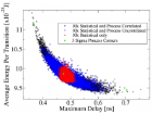
Circuit simulation is essential for functional logic verification, timing closure and power analysis – a combination which can allow circuit yield estimation, an important metric in determining the success of a design and profitability of a product. Timing closure, states that if maximum latch-to-latch delay in a system is D, with clock period T and latch setup time L, in order for a system to fulfill timing requirements, the maximum delay (often extracted by predictive simulation) is: D=T-L.
In the presence of variability, D becomes a statistical distribution, as variable MOSFET performance causes variable delays within a system. This distribution can be explored using statistical circuit simulation and used to predict yield. Similar analysis can be performed upon the power performance of a circuit (ideally simultaneously), and a distribution for power performance can be extracted. The correlated distributions for delay and power can be combined to provide Power-Performance(delay)-Yield (PPY) trade-off information which can determine the practical viability of a design and aide in the optimization/redesign strategy of a system.
The aim of our work is to investigate ways to propagate device level variability information to designers so as to provide power/performance and yield predictions to inform and aid design and design evaluation process.
Process Simulation
Professor Asen Asenov, Professor Scott Roy
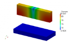
Typically an Integrated Circuit (IC) is fabricated by hundreds of sequential process steps, including lithography, etching, deposition, oxidation, ion implantation, diffusion, etc. TCAD (process and device simulation) provides deep insight into the device performance and information of how certain production processes influence the device behaviour, which is very important for IC production.
With emerging device architecture such as FinFETs, and requirement of complex channel profiles in bulk device to adjust the threshold voltage beyond the 50 nm gate length, conventional 1D or 2D TCAD simulations are not applicable. For reliable process simulation of FinFETs, state-of-the-art 3D simulation techniques are needed for critical process steps including ion implantation, diffusion, strain engineering etc. We are developing reliable, accurate and concise process simulation tools, most importantly for doping profiles and strain distribution within the device, forming the bases for accurate prediction of device performance and structure and process optimization.
Molecular Electronics
Professor Asen Asenov, Dr Vihar Georgiev, Professor Scott Roy
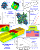
Our M-MOS Project (Molecular-Metal-OXide-nanoelectronicS: Achieving the Molecular Limit) gives us the exciting opportunity to research the ever-broadening field of molecular electronics. In particular, we investigate the viability, scalability and variability of a non-volatile flash-memory cell, in which the charge-storing component is a layer of polyoxometalate molecular clusters (POMs).
The idea is to utilise the highly attractive redox properties of the POMs -- they are multiply and reversibly reducible, which could facilitate multi-bit storage per transistor-cell. The small size (~1nm) of the POMs, and the variety of their structure, that can be controlled via chemical synthesis and determines their electronic properties, makes them attractive for memory applications.
The project is interdisciplinary, involving chemical synthesis and experimental characterisation of the POMs (X-Ray, ESI-MS, cyclic voltammetry, etc), DFT modelling of their electronic properties, device-level modelling and simulation of the Flash-Cell, and reflects a collaboration between the Schools of Engineering and Chemistry.
Fundamentally, we aim to establish a link between the two traditionally distinct fields of molecular design and modelling, and device design and modelling, and to exemplify the synergy derived from the diverse expertise held at each side.