Micro- and Nanotechnology
The Micro- and Nanotechnology Group delivers both fundamental and commercially-driven leading-edge research across a number of fields, including nanofabrication; electronic materials and devices; micro- and nano-mechanical systems (MEMS and NEMS); electronic circuits and systems; integrated sensors; and radiofrequency, microwave and terahertz technologies. Micro and Nanotechnology research teams use the James Watt Nanofabrication Centre and the Electronics Design Centre.
Research topics
Quantum CircuitsUltrafast SystemsSemiconductor Devices
Nano-Electronic Diamond Devices and Systems
Microsystem Technology
High Frequency Electronics
Electromagnetics Design
Bendable Electronics and Sensing Technologies (BEST)
Atomic Force Microscopy
Thermoelectric Systems Magnetoelectronics
Staff
| Dr Qammer Abbasi | Dr James Grant | Dr David Moran | |
| Dr Mohammed Al-Rawhani | Dr Phil Dobson | Dr Hadi Heidari | Professor Douglas Paul |
| Dr James Beeley | Dr Khaled Elgaid | Dr Ata Khalid | Dr Vincenzo Pusino |
| Dr Sung-Jin Cho | Dr Francesco Fioranelli | Professor Andy Knox FRSE | Dr Antonio Samarelli |
| Professor David Cumming | Dr Kevin Gallacher | Dr Xu Li | Dr Gary Ternant |
| Professor Iain Thayne | Dr Srinivas Velugotla | Dr Jue Wang | Dr Edward Wasige |
| Professor Jonathan Weaver | Professor Martin Weides |
Quick Links
Quantum Circuits
Our main research interest lies in coherent nanoelectronics, with a focus on quantum spintronics, hybrid qubit systems and quantum computing, simulation and sensing with superconducting quantum circuits.
Further information can be found on the group webpages:
Ultrafast Systems
Dr Khaled Elgaid, Dr David Moran, Dr Xu Li, Professor Iain Thayne, Dr Edward Wasige
The Ultrafast Systems Group conducts research into advanced semiconductor transistor design; ultra-high frequency and ultra-low power monolithic integrated circuit design; manufacture of transistors and integrated circuits with critical dimensions below 50 nm; and broadband on-wafer component test and measurement
Our work has applications in areas including III-V MOSFETs for digital circuits beyond the ITRS 22 nm technology generation; ultra-low power radio transceiver design and realisation for autonomous distributed sensor networks at 6 GHz and 24 GHz; and low noise mm-wave receiver design and realisation for 94 GHz and beyond imaging and sensing.
To be fully exploited, these application areas require low cost, high performance electronic components based on advanced, manufacturable transistor and integrated circuit technologies. We are addressing these issues by developing GaAs and InP HEMT and MOSFET technologies with gate lengths down to 15 nm. These next generation transistor technologies will eventually supersede our current monolithic integrated circuits based on 50 nm gate length transistor technologies operating from 6 GHz to 200 GHz.
Further information:
- Ultrafast Systems
Semiconductor Devices
Professor Douglas J. Paul, Dr Kevin Gallacher, Dr Lourdes Ferre Llin, Dr Muhammad Mirza, Dr Derek Dumas, Dr Richard Middlemiss, Dr Ross Millar, Dr Anwer Saeed, Kirsty Rew, Dr Richard Taylor and Dr Euan McBrearty
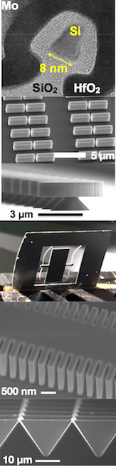
The Semiconductor Device Group undertakes a wide range of projects and presently has circa £18M portfolio of grants funding projects on quantum technology, single photon detectors, quantum devices, energy harvesting, photonics, quantum cascade lasers and mid-infrared sensor projects. All the projects involve the design, fabrication and characterisation of discrete or integrated devices or systems produced in the James Watt Nanofabrication Centre. We have, or are developing, a number of technology platforms which includes 8 nm diameter silicon nanowires, direct bandgap Ge and GeSn on silicon, n-Ge mid-infrared plasmonics, MEMS gravimeters, locked DFB lasers for rubidium cold atom systems and silicon photovoltaics. The Group has significant characterisation equipment available including Bruker vacuum FTIRs with mid-infrared and THz detectors; ball and die bonders; micro-Raman confocal microscopes for strain measurements; variable angle ellipsometers for optical parameter extraction; narrow linewidth Ti:Sa lasers for quantum technology; red diode laser LIV and linewidth characterisation; 10 fs Ti:Sa laser for THz generation and detection; tunable telecoms lasers; time correlated single photon counting lasers, electronics and detectors; 4.5 µm quantum cascade laser (CW and pulsed); 7.8 to 11.5 µm tunable quantum cascade laser; CW and ns pulsed CO2 lasers; 1 K cryostat with a 12 T magnet; AC and DC electrical characterisation (lockins, SMUs, voltage sources, current preamps, ...); a cryogenic probe station; two optical cryostats; a calibrated Newport solar simulator; and significant expertise in characterising devices. The group collaborates internationally with many top research groups around Europe and in North America and presents results at many different international conferences every year. The main application areas being developed are:
- 1. Chip-scale integrated cold atom systems for atomic clocks, rotational sensors, inertial sensors, quantum navigators, magnetometers and gravimeters;
- 2. Mid-infrared silicon quantum photonics (including SiGe, Ge, GeSn and SiGeSn) for security applications (explosives detection plus chemical and bio-weapons detection), environmental monitoring (gas detection) and personal healthcare sensors;
- 3. Short wavelength infrared and mid-infrared Ge on Si single photon avalanche detectors for automotive LIDAR, quantum optics, quantum communication and quantum information processing;
- 4. Si nanowire transistors for current standards, quantum sensors, biochemical sensors and quantum information processing;
- 5. Ge on Si quantum cascade lasers for applications in terahertz science and technology - especially oncology (skin cancer imaging);
- 6. Thermal photovoltaics using silicon photovoltaics for combined heat and power energy harvesting systems;
- 7. Ge mid-infrared plasmonics for integrated, temporal sensing applications;
- 8. MEMS gravimeters for petrochemical prospecting, geological surveys, early volcano warning systems, security applications and under road utility detection in cities. This work is in collaboration with Giles Hammond in the School of Physics & Astronomy.
Further information: Semiconductor Devices Web Pages
Nano-Electronic Diamond Devices and Systems
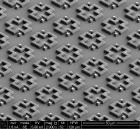
Beyond its allure as a rare gemstone, diamond possesses several unique and extreme properties which make it highly desirable as an engineering material for the development of a range of new and exciting technologies. It has the highest thermal conductivity of any bulk solid which allows heat to flow through diamond easier than any other material. It also has a large electronic bandgap of 5.5 eV which allows diamond to tolerate high electric fields/ high voltage operation and potentially be used in hazardous and radiation intense environments. Diamond also has high intrinsic electron and hole mobility which allows electronic charge to travel through the diamond structure with relative ease, making it ideal for high frequency electronics.
The Nano-Electronic Diamond Devices and Systems group (http://nedds.co.uk/) specialises in the investigation of diamond for the development of various electronic and nano-scale applications. Our current areas of research include diamond transistors (FETs), high power diamond electronic components, diamond nano-imprinting, diamond micro and nano-electromechanical systems (NEMS & MEMS), and diamond based chemical and biological sensors.
Microsystem Technology
Dr Mohammed Al-Rawhani, Dr James Beeley, Professor David Cumming, Dr Luiz Gouveia, Dr James Grant, Dr Ata Khalid, Dr Vincenzo Pusino, Dr Srinivas Velugotla
The Microsystem Technology Group researches and develops a wide range of leading-edge technologies including combined electronic sensor and imaging systems; medical diagnostic devices; integrated single-chip CMOS sensor devices; sensor and imaging arrays; wireless sensors; terahertz technology and systems; and control and data processing of hardware and software for sensor systems.
Our research work makes full use of the analogue/digital/mixed signal VLSI design and test facilities of the Glasgow Electronics Design Centre, and the custom device fabrication facilities of the James Watt Nanofabrication Centre. We collaborate extensively with engineers, biotechnologists, medics, vets, and computer scientists at a number of other UK and overseas universities. We are also supported by a number of leading multinational companies. Our work continues to attract extensive funding and support from both government research bodies and leading electronics companies.
Further information can be found on the group webpages:
- www.gla.ac.uk/mst
High Frequency Electronics
Dr Sung-Jin Cho, Dr Jue Wang, Dr Edward Wasige
Research in the High Frequency Electronics (HFE) Group at the University of Glasgow focuses on advanced electronic device technologies and associated integrated circuit design for the microwave, millimeterwave and terahertz (THz) frequency bands, and the integration of these with other physical domains to achieve new system functionality. Presently, we are developing new types of gallium nitride (GaN) based transistors for power electronics and for radio frequency (RF) applications, with funding from the UK Ministry of Defence (MoD), Defence Science and Technology Laboratory (DSTL), for the development of GaN based microwave power amplifiers (contract DSTLX-1000064098) and from the Engineering and Physical Sciences Research Council (EPSRC) for GaN based energy efficient power devices (grant EP/K014471/1). We are also developing compact electronic THz sources based on resonant tunneling diode technology with EPSRC-funding (grant EP/J019747/1). All our fabrication is carried out in the James Watt Nanofabrication Centre (JWNC), while all device/circuit characterisation within the Electronic Design Centre. The group works in collaboration with several academic and industrial partners.
Further information:
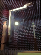
Electromagnetics Design
The Electromagnetics Design Group are an applied electromagnetics research group, with particular interests in the modelling, design and characterisation of new digital imaging pixels, optical plasmonics, magneto-plasmonics, terahertz metamaterials, micromagnetics, millimetre-wave and microwave antennas (including automated spherical near field antenna range), as well as solid state microwave synthesis, millimetre-wave smart labels for brand protection and the development of parallel ADI-FDTD algorithms.
Further information:
- Electromagnetics Design
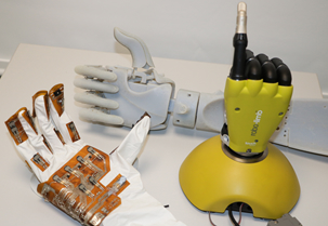
Bendable Electronics and Sensing Technologies (BEST)
The BEST group's multidisciplinary research interests include Flexible and Printable Electronics, Electronic Skin, Robotic Tactile Sensing, and Micro/Macroelectronics and System Integration.
The group focus on developing high-performance and cost-effective electronics and sensing systems on flexible substrates to enable tools, such as electronic skin (also known as tactile skin, smart skin or synthetic skin), which is of burgeoning interest in robotics, prosthetics, healthcare, wearable systems, and surgical instruments. Through integration of different types of sensors and electronics on flexible substrates, the electronic skin concept can also be extended to many other applications such as rollable sheets of solar cells or bendable photonics.
Further information:
- BEST
Atomic Force Microscopy
Dr Phil Dobson, Professor Jonathan Weaver
The AFM and Hyperlithography group builds on long-standing expertise at Glasgow in the area of electron-beam lithography.
The first strand of the work is concerned with the functionalisation of AFM probes. In this work, the AFM itself is used primarily as a vehicle to allow a lithographically defined sensor to be positioned close to, or in contact with a sample. Using this technique many contrast modes can be devised by simply choosing the sensor type to be made.
Hyperlithography is concerned with the desire to drive the size of structures down to the level at which lithographic objects become commensurate with natural objects, such as large molecules, typical of biological systems. The resolution of conventional electron-beam lithography is typically around 10nm for an isolated shape. Our hyperlithography allows the definition of very small gaps and wires, with significant dimensions down to 1nm or below. Using this capability we are working towards new sensors and instruments.
Further information:
Thermoelectric Systems
Professor Andy Knox
The group has a strong applications and industrial focus and deals with thermal, and electrical energy conversion systems.
Research themes include power electronics, test and characterisation of thermoelectric devices, simulation of dynamic thermoelectric systems, heat exchanger design, and energy conversion applications (including waste heat recovery, heat pumps, heat storage and phase change materials, Rankine cycle enhancement with THPs, solar thermal systems).
Further information:
Magnetoelectronics
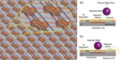
The Magnetoelectronics lab aims to promote and support engineering and physical science research in magnetism, magnetic sensors, circuits, devices and spintronics. Research in magnetism is broad ranging from theoretical, simulation, design and experimental work in fundamental physics to applications of magnetic devices, sensors and electronics.
We are working on sensors compatible with CMOS IC technology, allowing them to be manufactured with integrated electronic readout, produced in mass quantities (potentially at low cost), and deployed in a one-time use, disposable format for point-of-care testing. In this regard, various magnetic sensors including Hall effect sensors, Giant Magnetoresistance (GMR), Anisotropic magnetoresistance (AMR), Tunnelling magnetoresistance (TMR), spin valve sensors, SQUID sensors, magnetic resonance sensors (NMR, ESR etc.). Furthermore, we research on the magnetic tweezing to trap and manipulate the magnetic tags with a magnetic field to potentially speed up the reaction or remove unbound tags. Our study also focuses on in-depth analysis using simulation as it’s essential to ensure the correct targeted functionality.
Further information: