

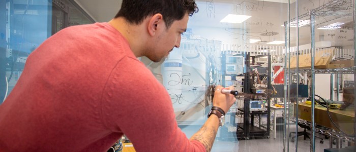
Electronics and Nanoscale Engineering
We are pioneering advancements in Electronics and Nanoscale Engineering, focusing on cutting-edge research in microelectronics, quantum systems, and photonics. Our work drives innovations in sensing, telecommunications, and quantum technologies, with applications spanning industries from healthcare to telecommunications.
The Electronics and Nanoscale Engineering Research Division, headed by Professor Stephen Sweeney, is organised into three primary research clusters each focusing on cutting-edge areas of technology.
Collectively, these clusters encompass research areas such as sensors, telecommunications, quantum technologies, terahertz and millimetre wave technology, advanced microelectronic devices, device simulation, metrology, and instrumentation.
Take a look below to explore our research clusters.
Head of Research Division
Useful links
- Our staff
- Publications
- PhD opportunities
- CDT Applied Photonics
- CDT Future Ultrasonic Engineering (FUSE)
- CDT Photonic Integration and Advanced Data Storage (PIADS)
UKRI Centres and Hubs
Our impact and legacy
With over 30 years of excellence in micro- and nanofabrication, our division's research leads to significant technological advancements with real-world applications, including:
-
Quantum Sensors: Developing materials and devices for demanding sensing applications, such as single-photon detection in the infrared spectrum. These technologies have applications in atmospheric remote sensing, astronomy, and quantum cryptography.
-
Nanofabrication: Our James Watt Nanofabrication Centre houses nanofabrication tools supporting extensive research grants and quantum technology hubs.
Industry and collaboration
The Electronics and Nanoscale Engineering Research Division collaborates extensively with industry partners, research institutions, and government bodies to drive real-world applications of our research.
Our work in quantum technologies, advanced sensors, and photonics has led to impactful partnerships across sectors such as telecommunications, healthcare, and energy.
We play an active role in national and international research initiatives, working alongside leading companies to develop cutting-edge devices and systems.
By fostering these collaborations, we ensure our innovations are not only at the forefront of academic research but also address pressing industry challenges and contribute to economic growth.
Our Research Clusters and Centres
We are actively looking to recruit new people for our diverse and inovative Research Clusters and Centre. Please contact specific clusters or centres below for more information and ongoing positions in your area of interest.
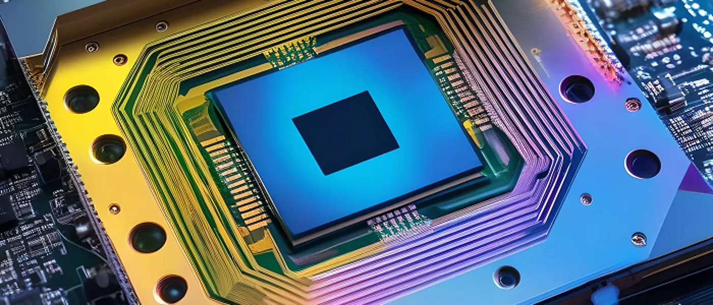
Electronics
Specialising in advanced semiconductor materials and devices, our research aims to develop technologies for electronic, sensing, and quantum applications.
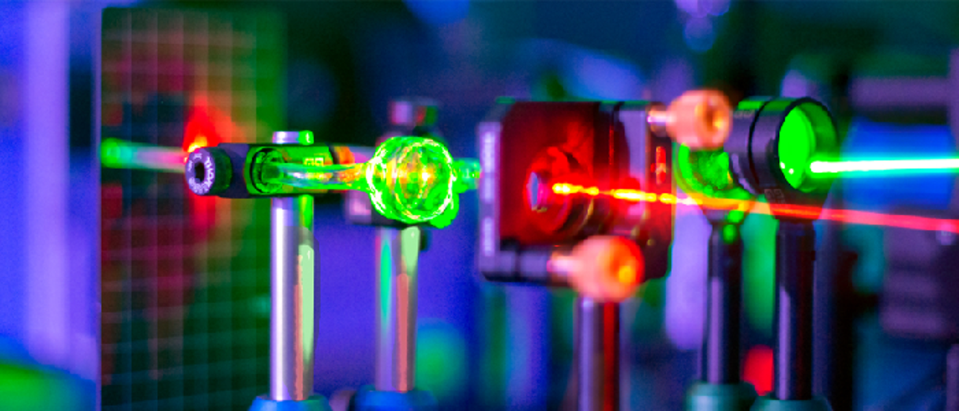
Photonics
Our work in photonics involves the development of high-speed optical devices and systems, contributing to advancements in communication and sensing technologies.

Quantum & Nano
Our work connects quantum technology with condensed matter and material science, focusing on superconducting spintronics, quantum engineered nanoelectronic circuits, and quantum information processing.

ANALOGUE - Semiconductor Packaging Facility
ANALOGUE is a state-of-the-art facility offering a fully automated semiconductor processing platform, from devices to applications, with integrated workflow design, data collection, and real-time analytics.