

Previous Projects
Previous Projects
The Detector Development group has been active in many projects in the past. Some of the more significant, but now ceased, projects are listed below:
GEMS
GaAs
ILC CCDs
Active Pixel Sensors
Active Pixel Sensors
Since the 1970's, CCD have primarily been the pixel detector of choice for the detection of visible light. However, in the last 2 decades, CMOS Active Pixel Sensors (APS) have increased both in terms of usage and functionality. Initially, APS-based devices suffered from a number of problems, including high readout noise, fixed pattern noise (FPN) and a limited dynamic range.
Despite these disadvantages, APS devices show much promise. Work on the design and fabrication of APS has led to continual improvement in the technology. Lower power consumption, lower cost, random access, and selective readout are now fully developed functions for CMOS sensors. The possibility of incorporating on-chip functionality such as analogue-to-digital conversion (ADC), timing logic for thresholding, and gain adjustment, is now driving an increased interest in these devices both in the scientific community and in the commercial sector.
Fig 1 (right) - 3T model for Active Pixel Sensors
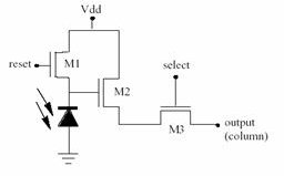 CMOS active pixels sensors (APS) are integrating sensors. The sense method for such devices depends on the measurement of the charge integrated on a photoelement (i.e. photodiode capacitance). APS incorporates at least 3 transistors per pixel: a reset transistor that resets the photo element, a source follower input transistor that converts the accumulated photo charge to voltage (the term 'active' in this instance refers to the incorporation of an amplifier within each pixel), and a row select transistor that selects the row to be read. Such circuits operate by resetting the photo element, allowing charge to accumulate and then sensing the charge value. The readout is column-parallel.
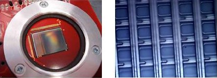
Fig 2 (below) - Pictures of Vanilla - a 520x520 25 um2 APS
 In collaboration with the RAL microelectronics group, Glasgow is designing and testing APS for particle detection for future PPE experiments.
Gem Detectors
Gem Detectors
The initial aim of the project is to complete the development of GEM-like structures from solid semiconductor materials like Si or SiO2. This technology will then be used to produce position sensitive micro gas detectors.
The use of a highly amplifying photosensitive front end for an existing pixellated detector e.g.. a CCD (charge coupled device) or APS (active pixel sensor) detector would increase the operational range further in to the UV while simultaneously allowing detection of ultra low energy X-rays from a very small number of photons.
Benefiting from the availability of in house semiconductor fabrication equipment and design technology the intermediate goal of this project is to produce readout chip specific GEM like micro-gas detectors. These would be designed to give each pixel in the array its own pre-amplifier. Finally after development of readout chip specific GEM foils, the ultimate integration of this technology will be to produce integrated GEM foils as part of the readout chip designing the structure developed earlier onto the upper metal layers of a standard CMOS process. This will allow amplification for individual channels in a small volume with high positional accuracy.
The Detector Development Group at Glasgow has contributed to many projects making use of many of the technologies that are proposed here. These include design and fabrication of "3D" detectors and existing work on the development of semiconductor GEMs. 3D detectors use vertical electrodes produced by DRIE (deep reactive ion etching) to produce semiconductor detectors with a large detection volume but a small drift distance between electrodes. As a result of this work there is already considerable expertise available in the field of DRIE. Figure 1 shows a series of deep etched holes in Si created using a Surface Technology Systems ASE (advanced silicon etcher) ICP (inductively coupled plasma) reactor. Figure 2 shows a top view of an array of 80 mm holes etched using the same process illuminated from the bottom. Additional experience gained during this work including surface passivation, metallisation, and pattern transfer will all prove invaluable to the progress of this research program.
Gas Detectors
Gas Detectors
Gas detectors depend on ionisation created by the interaction of incident radiation with the molecules in a gas volume. This creates ion-electron pairs. By applying an electric field the charged particles drift toward the electrodes giving rise to a signal. The amount of charge collected is related to the energy of the incident radiation and the charge it carries. This can make it difficult to detect fast moving lightly interacting particles due to the very small number of ion-electron pairs created. As a way to increase the signal detected the avalanche effect is exploited.
The avalanche effect is a consequence of increasing the electric field between the collecting electrodes. At low field levels the electrons and ions drift towards their respective electrodes, en route experiencing many collisions. The low mobility of ions means they have a gain little energy between collisions. Electrons on the other hand have a high mobility, and if the energy gained by an accelerated electron is higher than the ionisation potential a secondary free electron can be created by a collision. This secondary electron will also be accelerated and may cause further secondary ionisations. By applying a field ~106 V/m it is possible to get a sustainable avalanche in a typical detector gas mixture.
Existing types of micro-patterned gas detectors utilise the avalanche effect to amplify very small signals, however they generally have a drift length of several mm. The drift distance allows the generated electron cloud to diffuse causing loss of signal and loss of spatial resolution due to stimulation of nearby channels by charge sharing.
GEM foils produce amplification by producing a strong electrical field between the front and back surfaces of a pierced insulating substrate material, commercially available devices are made from kapton. Figure 3 shows a schematic of a GEM foil. The avalanche takes place in the region of the holes were the field lines are closely packed allowing an increased gain.
Wide Bandgap Materials
Wide Bandgap Materials
For the past 50 years silicon has been the semiconductor material of choice for physicists involved in particle and photon detection experiments. The shortcomings of silicon, for example its poor radiation hardness and low signal to noise ratio (SNR) in the UV region of the electromagnetic spectrum, have led to increased interest in other semiconductor materials such as Silicon Carbide (SiC) and Gallium Nitride (GaN). SiC and GaN are called Wide Bandgap Semiconductors on account of their large bandgaps in comparison to silicon.
The Glasgow group investigate the performance of various SiC and GaN materials as radiation hard particle detectors. Also investigated within the group are GaN UV detectors for applications in protein crystallography experiments.
ILC CCDs
ILC CCDs
Glasgow was involved in the development of CCD detectors for the UK international linear collider collaboration LFCI. The work on CCDs involved the modelling of radiation damage and the testing of devices. Work on mechanics was due to start but ceased due to ILC funding problems within STFC.
GaAs
GaAs
There were two main drivers for the GaAs research that was performed in the Glasgow detector development group, namely; PPE and medical imaging.
Originally the group's interest was focused, within and leading the CERN RD8 collaboration, on the development of radiation hard detectors to replace silicon at the inner most radius of the forward ATLAS semiconductor tracker, (SCT). However, after much successful development of GaAs as a particle detector the charge collection efficiency was shown to degrade significantly after a high radiation exposure. Therefore GaAs was removed from the SCT and replaced with Silicon sensors.
The second area of interest was in medical and dental imaging. Epitaxial GaAs material was developed as part of a EU frame-work 5 programme (XIMAGE) and further developed as part of a frame-work 6 programme (CANDID). These activities saw significant developments in material properties (thicker epitaxial layers, improved charge collection efficiency). However, at present the group does not have an active research programme in GaAs.