3D and active edge detectors
3D and active edge detectors
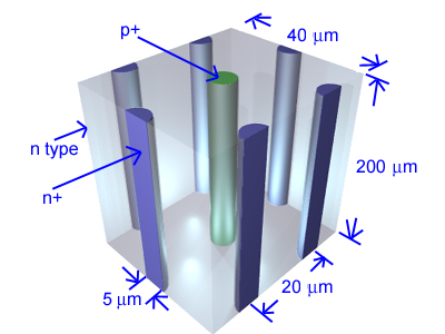
 The 3D detector consists of etched holes normal to the surface of the silicon, a few microns in diameter with a depth equal to the silicon wafer thickness. These are filled with doped poly-silicon to form interposed arrays of n+ and p+ columns. The electric field is between the columns, and deposited charge from inozing radiation is collected parallel to the device surface. The charge carriers therefore travel only the distance between the holes, not the full material thickness resulting in the collection distance being a user-defined parameter and independent of the detector thickness. A small extension of the technology allows the edge of the detector to be etched from the wafer and doped. This forms an active edge, with no saw defects, that contains the electric field. Such a device has been shown to be active to within 5um of the physical edge of the device.
Benefits
Benefits
The 3D structure makes it possible to place the detector's electrodes close together without having to reduce the thickness of the detector. This has a variety of benefits. By reducing the distance between electrodes by a factor of 10 (from 200 to 20 microns) the collection distance can be reduced by a factor of 10 and the depletion voltage can be reduced by a factor of 100. The reduced collection distance reduces charge loss, via trapping, in an irradiated device and increases the signal speed. Due to the contained nature of the pixel, charge sharing is reduced. The active edge device implies that individual detectors can be close-packed without inactive material between unit cells, thereby reducing the mass of tracking detectors and the dead areas in imaging devices.
3D detectors provide fast response, a small dead area, and radiation hardness. These advantages mean that promising applications include: tracking using silicon detectors at the upgraded Large Hadron Collider (sLHC), medical imaging, and synchrotron light sources.
Collaborators
Collaborators
The Glasgow group works with several collaborators - industrial as well as academic - in the development and explotation of 3D detectors, including:
- IceMOS Technology LTD (Belfast, NI, UK)
- Centro Nacional de Microelectrónica (IMB-CNM, CSIC) (Barcelona, Spain)
- The Diamond light source Ltd (South Oxfordshire, UK)
- Fondazione Bruno Kessler, FBK, Microsystems Division (Trento, Italy)
- ATLAS Pixel upgrade collaboration
- The CERN RD50 collaboration
- University of Freiburg (Germany)
- Previous collaborations
More information on the 3D project at Glasgow is available from the Local Glasgow 3D Active edge detector pages
Contact: Richard Bates

