Research
Photonics
Optoelectronics is one of the longest established research activities in the University of Glasgow. The broad range of fabrication technologies and diverse tool set supports work across a range of materials systems including III-V semiconductors, silicon, superconductors, glass and polymers.
Optoelectronic and photonic integrated circuits developed at the JWNC support research in areas of gas sensing, telecommunications, atomic cooling, terahertz signal generation, LIDAR, single photon detectors and focal plane array detectors.
As an example, precision electron beam lithography is used to fabricate devices such as DFB lasers with complex chirped and phase shifted gratings. The gratings can be tailored for applications such as high-speed direct modulated lasers for communications, high-power eye-safe lasers for LIDAR and narrow-linewidth lasers for atomic cooling.
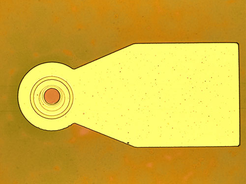
780 nm DFB lasers for Rb cold atom systems
Quantum Technology
The JWNC is delivering devices and circuits to all four UK Quantum Technology Hubs for applications in quantum communications, quantum sensing, quantum imaging and quantum computing. Technologies being delivered include short-wave infrared single photon detectors and imaging arrays, DFB lasers for cold atom systems (atomic clocks, quantum navigator, magnetometers), photonic integrated circuits (cold atom sources, entangled pair sources, frequency combs), MEMS vapour cells, grating magneto-optical traps, microfabricated ion traps, silicon nanowires and quantum dots and superconducting qubit circuits.

Energy Efficient Electronics
The JWNC is currently supporting projects in gallium nitride-based RF and power transistors for high efficiency communications and high temperature power conversion, indium phosphide based RF terahertz circuits for beyond 5G communications and radio astronomy, gallium arsenide based transistor read out integrated electronics for mid-infrared imaging arrays and indium gallium antimony based ultra-low power cryogenic RF transistors for quantum computing.
Security
Many of the technologies being developed within the JWNC have security applications including electronic or photonic sources and detectors, imaging arrays, single photon 3D lidar imaging systems, mid-infrared sensors for chemical-biological-explosives identification and position, navigation and timing devices. Examples of these technologies include single photon detectors and imaging arrays (geranium on silicon and III-V single photon avalanche detectors), mid-infrared antimonide imaging arrays and sensors, geranium on silicon mid-infrared spectroscopic sensors, chip scale atomic clocks, MEMS gravimeters, atomic magnetometers and quantum navigators.
Ge on Si SPADS & QKD
Medical Devices and Diagnostics
The fabrication capabilities of the JWNC are being used to create a range of diagnostic lab on a chip devices that provide cost effective, instantaneous ‘Sample-to Answer’ results. This work uses a variety of different material processing methods, developing devices by processing silicon, glass and polymer materials.
In the field of medical devices, such capabilities have underpinned a range of new applications including new methods for precision pulmonary drug delivery with aerosols, new ultrasonic dental drills, as well as smart stents that can react to a patients’ individual requirements. Microfabricated devices for surface acoustic waves are used to manipulate and sample biological materials.
Research on future applications involves developing neuro-technologies that interface directly with the brain to address conditions such as tinnitus, strokes and spinal injuries.
Research in nanoscale surface texturing of biomaterials has demonstrated the use of surface topography to achieve precise control of cell fate at very small scales and introducing a small amount of noise in the nanopatterns can stimulate stem cells to form bone.
Surface texturing is also used to manufacture chiral surface plasmon biosensors. Metamaterial devices with different chirality can detect the molecular structure of biomolecules, and other designs can verify the precise formulation of food and drink products important from a health safety perspective.
Sensors
Development of new types of sensors for the 21st century is being carried out using the unique expertise of the JWNC. Often combining electronics, photonics and micro mechanics within single sensors, new detection capabilities are being brought to healthcare, gas sensing, LIDAR, quantum imaging and gravity measurement. Photonic covers wavelengths from mid infrared to ultra violet and electronics covers frequencies up to the terahertz range. Micro fluidic and micro mechanical systems are fabricated with electronic and photonic readouts. The JWNC is the main manufacturer for a range of specialist probes for atomic force microscopes that are used in research facilities across the world.
Nanofabrication
Innovation in nanofabrication techniques and processes is the primary underpinning capability of the JWNC. The centre has led the way in developing processes that combine ground breaking techniques in, for example, electron beam and nanoimprint lithography, atomic level plasma processing, high vacuum deposition activity with metrology expertise. This has led to an extensive library of processing modules and background IP that combine photonics, electronics and micro mechanic expertise accelerating product development timescales.