

Technology Platforms
Integrated Photonics
The evolution into photonic integrated circuits (PICs) is the next logical step in the world of optics bringing massive performance benefits to fibre-optic communications, biomedical and health sensing, and quantum computing. The JWNC is a world leader in III-V photonics integrated circuits platforms supplemented by expertise in modelling and characterisation of devices in Gallium Nitride, Gallium Arsenide, Indium Phosphide and Antimonide materials and alloys and is pushing the boundaries of hybrid integrated optics in silicon and related materials. Expertise in hybrid integration includes integrating III-V lasers with silicon, silicon dioxide, and silicon nitride waveguides with devices being supplied to multiple hubs in the National Quantum Technologies Programme.
 Si Mid-infrared Photonics
Superconducting Quantum Technologies
Superconducting Quantum devices address the most demanding applications in single-photon detection, low noise electronics, quantum simulation and quantum computing.
The JWNC has world-class capability and expertise in the fabrication of superconducting materials and the creation of quantum devices and circuits. Thin film growth is carried out using UHV sputtering or atomic layer deposition and devices are patterned by photo- or electron beam lithography and dry etch. Testing and Failure analysis is supported via a full suite of advanced metrology and materials characterisation tools within the centre and advanced low temperature electrical, microwave and optical testing in the research labs of the James Watt School of Engineering. Much of the research and fabrication work undertaken in the JWNC supports the UK National Quantum Technology Programme including activity for the QuantIC, QComm and HQCS hubs with circuits also being supplied to industry partners.

Array of Josephson tunnel junctions
III-V Electronics
III-V based components have higher switching speeds, higher efficiencies, higher breakdown voltages and improved high temperatures performance compared to silicon and are key enablers in imaging, sensing, communication and computing applications.
The JWNC has extensive fabrication expertise in III-V electronics spanning nitride, phosphide, arsenide and antimonide based materials and has produced a wide range of amplifiers, high frequency power sources, frequency converters, and high sensitivity detectors with world leading performance. The centre is currently supporting III-V projects in gallium nitride, a transformative technology for delivering high power, high temperature and high energy efficiency applications in RF and power conversion and is pioneering gallium nitride on diamond devices. Projects are also ongoing in indium phosphide-based RF and mm-wave circuits for 5G communications and radio astronomy, gallium arsenide based transistor read out integrated electronics for mid-infrared imaging arrays and indium gallium antimonide based ultra-low power cryogenic RF transistors for quantum computing.
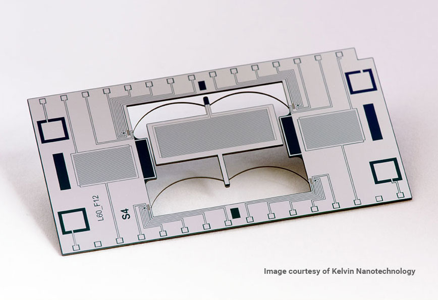
MEMS
Micro Electro Mechanical Systems (MEMS) are miniaturised electro mechanical devices that give the ability to sense, control and actuate on a micro scale. For example, MEMS accelerometers are widely used in mobile phones and gaming applications. Recently the JWNC has fabricated an ultra-sensitive accelerometer – Wee-g, the world’s first MEMS gravimeter with sufficient sensitivity to measure the Earth tides - deformations of the Earth caused by the daily tidal forces of the Moon and Sun. The JWNC created a transformative new fabrication technology for precision MEMS sensors and a wafer scale process enabling volume manufacture of MEMS gravimeters on-chip. The process involves photolithography and high aspect ratio deep-reactive ion etching of silicon, metallisation to produce on-chip heaters/thermometers for thermal control, and patterning SD2 glass to create a precision pickup electrode.
 Wee-g
Wee-g
Lab on a Chip
The integration of analytical sensing devices that enable low volumes of liquid samples to be processed and measured is often referred to as Lab-on-a-Chip (LOC) technology. These miniature systems which reduce analysis costs and decrease analysis times have applications in areas like infectious disease diagnosis or process monitoring. LOC systems generally work by pushing a liquid sample through a microfluidic device, using either mechanical pressure or electrokinetics. In disease diagnosis, we have developed new techniques to actuate pressure driven flow, using ultrasonic waves. A finger prick volume of blood is pushed through a chip, which allows us to break open the blood cells and detect microbes from their DNA sequence through biochemical reactions.
The nanofabrication facilities of the JWNC are used to etch, machine, mould or emboss the microfluidic channels and the sensors they are connected to. This capability underpins research across a range of applications in medical and veterinary diagnostics and environmental measurement using a broad range of detection methods based upon electrical, electrochemical, optical, acoustic and thermal microsensors.
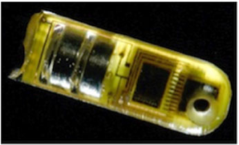 Lab on a pill
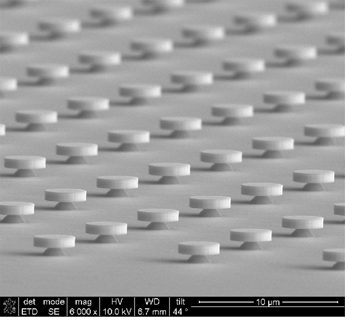
Functional Surfaces
Micro- and nanoscale surface texturing is a powerful means to change the interfacial properties of materials. Textured surfaces give materials unique attributes ranging from water repellence to strong adhesion and can be used to create patterns and scaffolds that promote cell growth allowing nerve repair and bone regeneration. Novel optical devices such as flat lenses and gratings for suspending single atoms in quantum applications are also fabricated using this approach.
The JWNC is at the forefront of surface texturing realised using electron beam lithography and reactive ion etching. The JWNC also has capability for volume production in this area via Nano Imprint Lithography (NIL) techniques which use injection moulding to implement surface texturing at a much higher throughput than can otherwise be achieved.
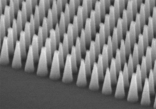 Motheye - Image courtesy of Kelvin Nanotechnology