

Process Capability
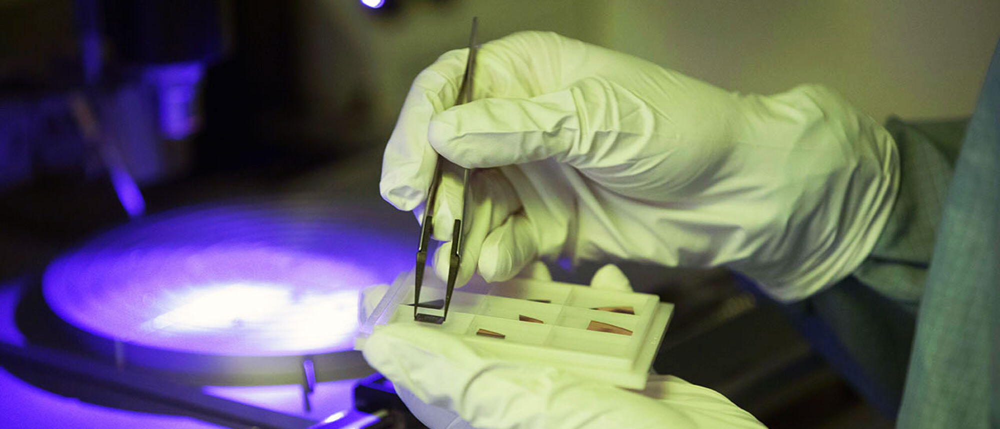
Lithography
Lithography is the process of writing patterns across a substrate. The JWNC has capability across electron beam lithography which delivers the smallest geometries and greatest flexibility, optical lithography with higher throughput but lower resolution and nanoimprint lithography which can achieve very small geometries, high throughput and can be used for 3D patterning.
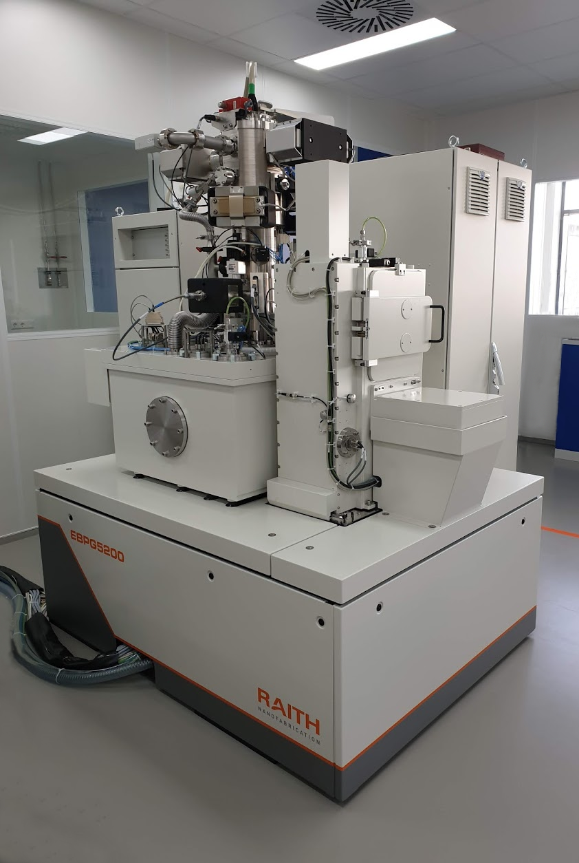
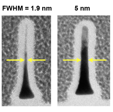
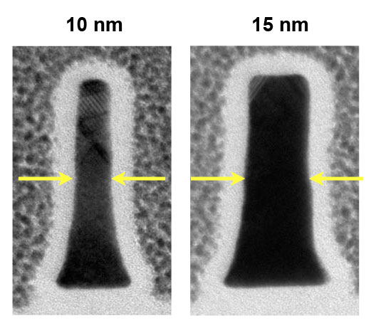
The Centre has three electron beam systems which process approximately 2500 jobs per year. These systems write over an area of 200mm routinely achieving 20nm stitch and alignment accuracy, and minimum feature sizes of 10nm. World leading precision in position, for instance sub-1nm alignment, and line widths down to 5 nm can be achieved for particular applications.
For optical lithography the JWNC also has three mask aligners with minimum linewidths down to 1 µm. Substrates of up to 8-inch diameter can be patterned with proximity, hard and vacuum contact modes.
Nanoimprint lithography can achieve feature sizes down to 20 nm.
These three lithography methods can be used together in a mix and match mode to optimize resolution and throughput dependent on batch size.
Plasma and Thermal Processing
The JWNC houses 14 plasma tools, comprising 5 deposition and 9 etching systems and processes around 7000 jobs per year.
Plasma assisted deposition of dielectrics such as silicon dioxide, silicon nitride and amorphous silicon use either plasma enhanced chemical deposition or inductively coupled plasma chemical vapour deposition, while metal oxides and nitrides are deposited using thermal or plasma enhanced atomic layer deposition.
Reactive ion etching and inductively coupled plasma tools are used with an extensive range of etch chemistries and recipes to etch micro and nano sized features on a diverse range of semiconductors, dielectrics and metals.
The JWNC also has the capability for growing thermal and wet oxides on silicon and low-pressure chemical vapour deposition of Nitrides on Silicon. These industrial scale furnaces can process up to 300 eight-inch wafers at a time.
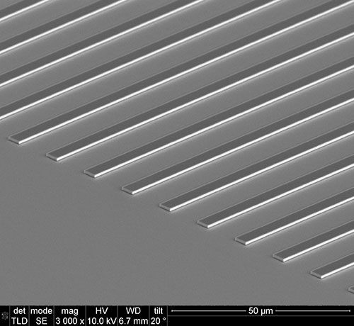 Ridge Array
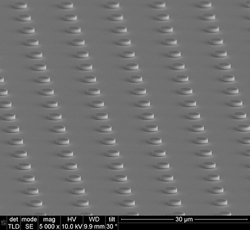 Disks Array
High Vacuum Deposition and Annealing
The JWNC is well equipped with a range of fully automated, recipe driven high vacuum deposition systems which can accommodate 4” and 6” wafers and diced substrates. The Centre has thermal evaporation, electron gun and magnetron sputtering systems. Many different materials can be deposited from metals and dielectrics to superconductors, and multiple layers can be deposited in a single run.
As an example, this technology has been used to give the JWNC a world leading position in Quantum Well Intermixing structures to produce advanced lasers.
The JWNC has rapid thermal annealers for sintering electrical contacts. Rapid heating and cooling allows diffusion of metals and other dopants to be targeted giving precise control over properties such as contact resistance.
 Dry O2 oxidation at 950 oC for 90 s > 4 nm SiO2
Metrology
Metrology is a cornerstone of modern nanofabrication and the JWNC has a comprehensive suite of equipment capable of characterising complete devices and those at interim stages of manufacture. The tool set includes electron and optical microscopes, atomic force microscopes, spectroscopy and electrical and thin film characterisation equipment.
A unique capability is an integrated vacuum cluster tool combining atomic layer deposition, plasma enhanced chemical vapour deposition and etching tools, with a scanning Auger / X-ray photoelectron spectroscopy microscope. This allows elemental mapping of surfaces with sub 10nm resolution.
III-V Epitaxy Growth
An integral part of the JWNC’s capability is its access to both molecular beam epitaxy for antimonide materials and metal organic vapour phase epitaxy for a wide range of III-V semiconductors. These systems are operated in conjunction with industry partners and include the capability of selective area epitaxy and overgrowth for photonic integration.