

Development of CMOS-Compatible High-Tc Niobium Nitride Josephson Junction Field-Effect Transistors on Silicon
Published: 3 July 2026
Yusheng Xiong, with support from Kaveh Delfanazari, is developing silicon-compatible CMOS-compatible gated niobium nitride, showcasing a scalable pathway towards Boolean logic circuits.
Josephson Junction Field-Effect Transistors (JJFETs) represent a promising beyond-CMOS device platform for ultra-low-power cryogenic Boolean logic. In this project [1], we developed CMOS-compatible gated niobium nitride (NbN)-silicon-NbN JJFETs directly on silicon substrates. Leveraging the advanced fabrication infrastructure at the James Watt Nanofabrication Centre (JWNC), we systematically optimized nanoscale patterning, superconducting film processing, and gate-stack integration to realize sub-100 nm channel devices.
The core achievement of this work lies in the precise fabrication of 33 nm Josephson junctions and 75 nm gated JJFETs using high-transition-temperature (high-Tc) NbN films deposited on silicon wafers.
To fabricate these devices, we employed a comprehensive suite of JWNC cleanroom facilities:
- Reactive magnetron sputtering for deposition of 90 nm NbN superconducting films with controlled stoichiometry and uniformity across the silicon wafer.
- Electron-beam lithography (EBL) for defining nanoscale junction gaps (down to 33 nm) and ultra-narrow gate structures with optimized exposure dose calibration.
- Inductively coupled plasma reactive ion etching (ICP-RIE) for anisotropic pattern transfer through the NbN film and controlled silicon over-etch.
- Atomic layer deposition (ALD) for conformal alumina (Al₂O₃) gate dielectric deposition, ensuring full sidewall coverage over etched NbN features.
A key contribution was the systematic electron-beam dose optimization for both junction and gate patterning. Dose matrices were implemented to compensate for proximity effects and lateral development, enabling reliable fabrication of 50 nm and sub-50 nm gaps. Finalized SEM inspections confirmed well-defined 75 nm channel lengths and uniform gate overlap with high structural fidelity.
This project showcases JWNC’s capability to deliver advanced superconducting nanoelectronics fully integrated with silicon-compatible fabrication processes. By combining superconducting materials, high-resolution lithography, and atomic-scale dielectric engineering within a CMOS-compatible framework, this work establishes a scalable pathway toward cryogenic Boolean logic circuits based on high-Tc NbN Josephson field-effect transistors.
The successful realization of nanoscale NbN JJFETs demonstrates not only the technical excellence of JWNC’s cleanroom infrastructure but also its critical role in enabling next-generation superconducting electronics research at the University of Glasgow.
[1] Xiong, Yusheng and Delfanazari, Kaveh (2026) Silicon-based Josephson junction field-effect transistors enabling cryogenic logic and quantum technologies. APL Engineering Physics, (Accepted for Publication).
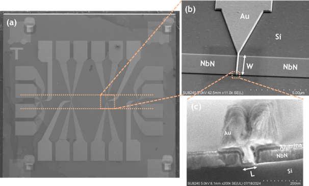
Figure 1. Scanning electron microscopy images showing (a) the overview of the chip with four Josephson junctions and the gates on each of them, and (b) the zoom-in view of one of the Josephson junction and the gate on top, with the junction width W=4um, and (c) the cross-section view of (b) showing the complete layers of the device with the junction length L=75nm.
First published: 3 July 2026