Tough materials, strong bonding - Electron microscopy applied to imaging bonded interfaces
Client: DSTL, Defence Science & Technology Laboratory
Service: FIB-SEM inestigation & sample preparation, TEM imaging of interfaces
Materials such as Silicon Carbide are extremely hard and light. However, complex shapes fabricated from many pieces are only as strong as the bonds joining them together.
The advantageous properties of these materials and their bonding together is of interest to the Defence Science and Technology Laboratory as part of a programme to promote improvements in ceramic armour efficiency within the UK Defence Industry.
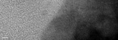
In a collaboration led by colleagues in the Institute for Gravitational Research (IGR) (who have pioneered the hydroxide-catalysis bonding of Silicon Carbide) we have investigated the starting material surfaces and subsequently the interfaces between bonded pieces. Transmission electron microscopy (TEM) has been used to image in cross-section, and at a range of lengths down to the nanoscale, the physical structure of the bulk materials and the surface layers upon which bonding depends. Further to this we have applied spectroscopic techniques to produce "maps" showing atomic elemental compositions of the various regions. This information has been fed into optimising the bonding process to produce the highest strength bonds when tested.