

Low-Loss Optical System on Lithium Niobate on Insulator Platform
Published: 10 February 2026
Zhibo Li explores the challenges of etching Lithium niobate and the potential for optimisation for use in quantum technologies and communications.
Lithium niobate (LiNbO3 or LN) has excellent optical properties, such as wide optical transparency window (visible to mid-infrared), low optical propagation loss, and strong electro-optic effect. These features make LN a valuable material across a broad range of applications, from optical communication system to emerging quantum technologies. Traditional optical LN devices are limited to standalone intensity or phase modulators which are based on the bulk LN material, with a typical device size of 10s cm. In recent decades, the maturity of lithium niobate on insulator (LNOI) material platform has not just seen more functionalities to be able to monolithic integrated on one chip but also shrink the overall device footprint into millimetre scale, highlighting its advantages in size, weight and power consumption (SWaP).
However, the design and fabrication of low-loss LNOI optical components and systems have yet to be fully investigated. For example, (1) the plasma etching of LN still remains challenging, because two commonly used etching chemistries, fluorine-based and chlorine-based gases, are not suitable in this case. Fluorine-based gases produce non-volatile LiF by products, resulting in rough etched surfaces and high optical losses. Chlorine-based gases cannot effectively react with LN, thus unable to achieve a decent etch rate; (2) process design kit (PDK) for LNOI photonic integrated circuits (PICs) is still under development, this requires a closed-loop of design, manufacturing, and testing process, with continuous iterations to achieve optimal device performance. In this project the main innovation points achieved are to address these issues aforementioned:
- Development of the whole fabrication process for patterning micro and nano features on LNOI, while achieving very low optical propagation loss (0.1-0.2 dB/cm or even lower) measured by cutback method.
- Completion in design and experimental verification of basic building blocks (e.g. waveguide system, micro-ring resonator, grating coupler, directional coupler, beam splitter and combiner, Mach-Zehnder interferometer) towards building various functional LNOI PICs.
So far, UoG is the only institution in the UK to conduct research activities on LNOI PICs. The design and fab capabilities developed here can be served as a generic process platform, providing multi-project wafer (MPW) runs for customised designs of LNOI PICs. Here I only show an example of compact LNOI waveguide Bragg gratings for tunable filter and fast modulator to be used in telecom area, but potential applications can be extended to onchip frequency comb, quantum key distribution, entangled photon-pair generation, et al., with applying different designs.
The tools involved in this project include: Raith EBPG 5200 ebeam lithography, OIPT Plasmalab System 100 ICP etching, OIPT PlasmaPro 100 PECVD deposition, OIPT System 100 ICPCVD deposition, and ebeam evaporator for metallization.
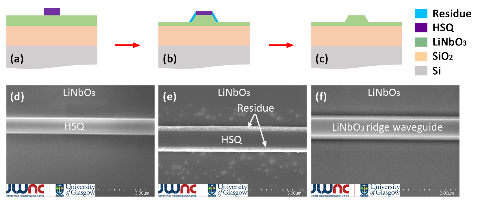
Fig.1, Process flow of low-loss optical systems fabricated on the LNOI platform, (a) nanoscale patterning by using the electron-beam lithography system, (b) modified plasma etching, (c) post wet etching and cleaning. The corresponding scanning electron microscope (SEM) images of these steps are shown in (d), (e) and (f) respectively. Surface roughness of the etched area in (f) is < 0.2 nm, measured by atomic force microscope (AFM).
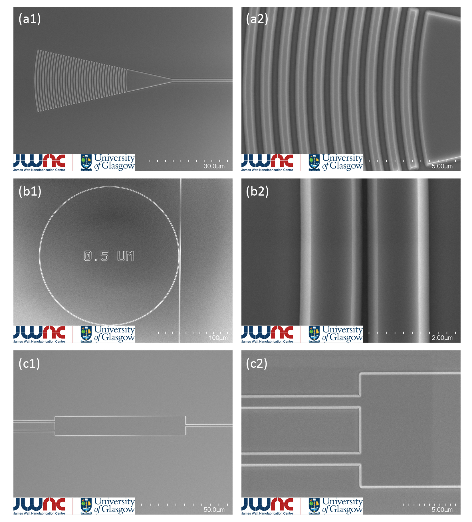
Fig.2, Examples of optical components towards LN PICs, (a1) & (a2) surface grating coupler, (b1) & (b2) micro-ring resonator, the coupling gap is ~500nm, and (c1) & (c2) multi-mode interferometer.
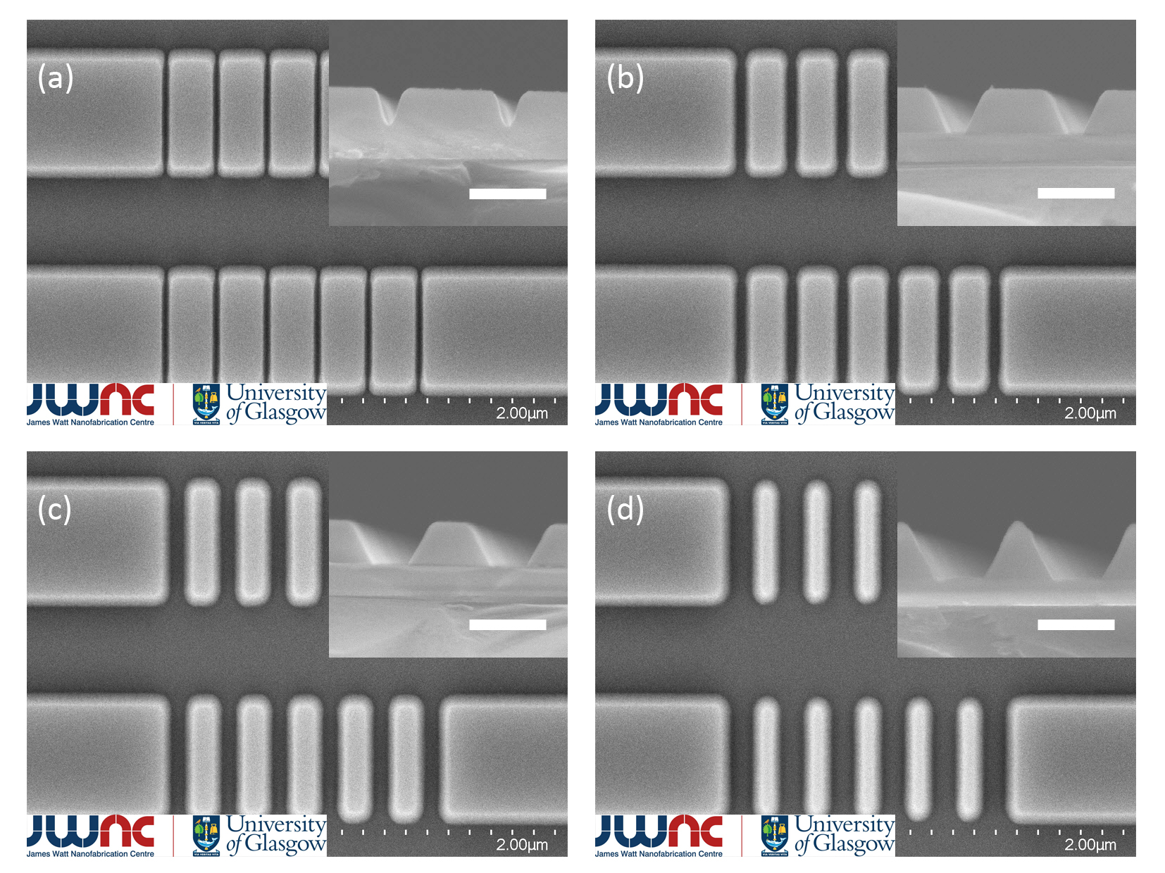
Fig.3, SEM images of Bragg gratings on LNOI with different duty cycles (mark-space ratios), (a) 80%, (b) 60%, (c) 40%, (d) 20%. The insertion in each figure shows the corresponding cross-section view from the grating region.
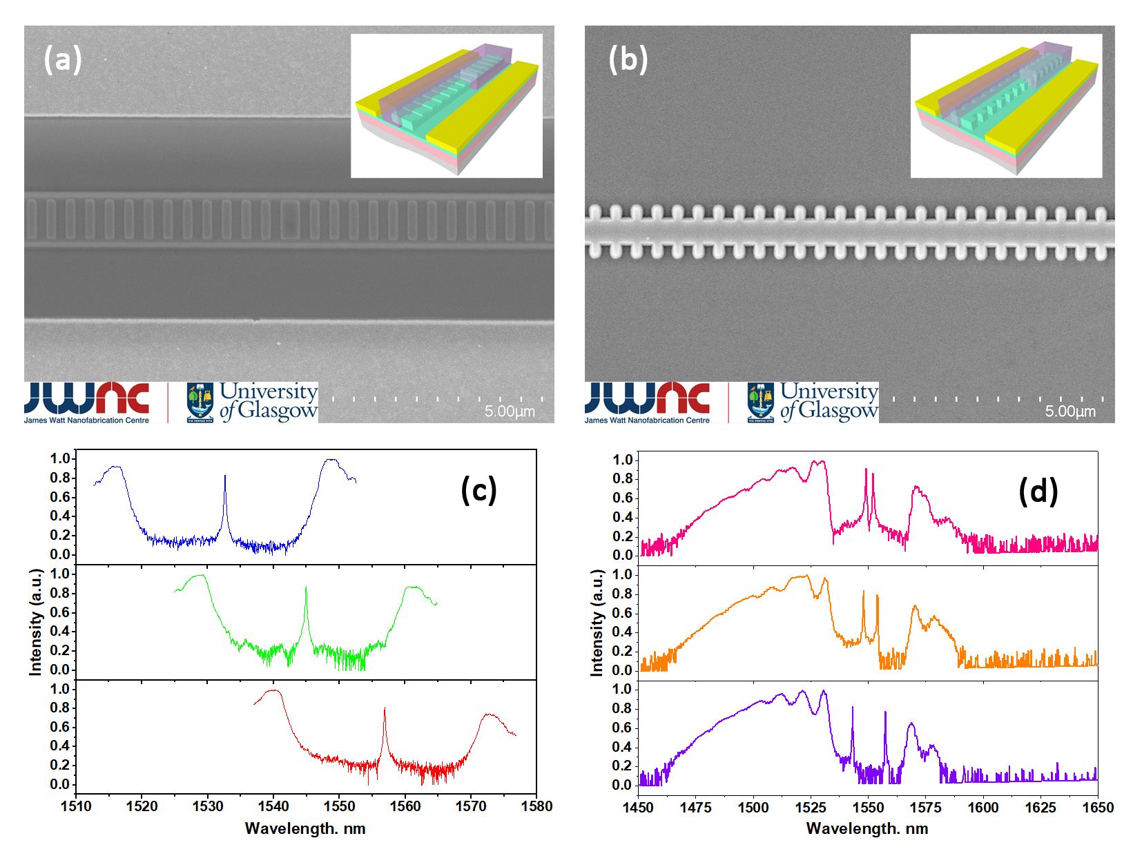
Fig.4, Two Bragg grating designs based on the LNOI platform for tunable filter and intensity modulator for optical communications, (a) buried grating, (b) sidewall grating, (c) and (d) optical transmission spectra for different grating designs.
First published: 10 February 2026