

New manufacturing process could be passport to flexible next-gen electronics
Published: 10 August 2021
A new method for manufacturing electronics which prints high-performance silicon directly onto flexible materials could lead to breakthroughs in technologies including prosthetics, high-end electronics and fully bendable digital displays.
A new method for manufacturing electronics which prints high-performance silicon directly onto flexible materials could lead to breakthroughs in technologies including prosthetics, high-end electronics and fully bendable digital displays.
https://youtu.be/GqkjDCHeVws
In a new paper published in the journal NPJ Flexible Electronics, engineers from the University of Glasgow’s Bendable Electronics and Sensing Technologies (BEST) group outline how they have streamlined and improved the conventional process for creating flexible large area electronics.
Until now, the most advanced flexible electronics have been mainly manufactured by a process called transfer printing, a three-stage stamping process a bit like receiving an ink stamp in a passport when visiting another country.
First, a silicon-based semiconductor nanostructure is designed and grown on a surface known as a substrate. In the second stage, the nanostructure is picked up from the substrate by a soft polymeric stamp. In the final stage, the nanostructure is transferred from the stamp to another flexible substrate, ready for use in bendable devices like health monitors, soft robotics, and bendable displays.
However, the transfer printing process has a number of limitations which have made it challenging to create more large-scale, complex flexible devices. Precisely controlling critical variables like the speed of transfer, and the adhesion and orientation of the nanostructure, makes it difficult to ensure each stamp is identical to the last.
Similar to how a badly-stamped passport can make it difficult for travellers to read, an incomplete or misaligned polymeric stamp onto the final substrate can lead to substandard electronic performance or even prevent devices from working.
While processes have been developed to make the stamping transfer more effective, they often require additional equipment like lasers and magnets, adding additional manufacturing cost.
The Glasgow team have taken a different approach, removing altogether the second stage of the conventional transfer printing process. Instead of transferring nanostructures to a soft polymeric stamp before it is transferred to the final substrate, their new process what they call ‘direct roll transfer’ to print silicon straight onto a flexible surface.
The process begins with the fabrication of a thin silicon nanostructure of less than 100 nanometres. Then the receiving substrate - a flexible, high-performance plastic foil material called polyimide – is covered in an ultrathin layer of chemicals to improve adhesion.
The prepared substrate is wrapped around a metal tube, and a computer-controlled machine developed by the team then rolls the tube over the silicon wafer, transferring it to the flexible material.
By carefully optimising the process, the team have managed to create highly-uniform prints over an area of about 10 square centimetres, with around 95% transfer yield – significantly higher than most conventional transfer printing processes at the nanometre scale.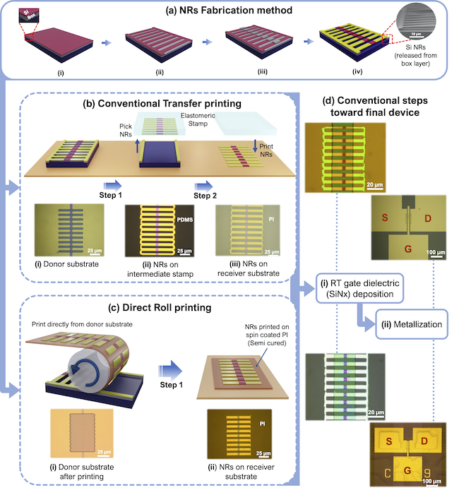
Professor Ravinder Dahiya is the leader of the BEST group at the University of Glasgow’s James Watt School of Engineering.
Professor Dahiya said: “Although we used a square silicon wafer sample of 3cm on each side in the process we discuss in this paper, the size of the flexible donor substrate is the only limit on the size of silicon wafers we can print. It’s very likely that we can scale up the process and create very complex high-performance flexible electronics, which opens the door to many potential applications.
“The performance we’ve seen from the transistors we’ve printed onto flexible surfaces in the lab has been similar to the performance of comparable CMOS devices – the workhorse chips which control many everyday electronics.
“That means that this type of flexible electronics could be sophisticated enough to integrate flexible controllers into LED arrays, for example, potentially allowing the creation of self-contained digital displays which could be rolled up when not in use. Layers of flexible material stretched over prosthetic limbs could provide amputees with better control over their prosthetics, or even integrate sensors to give users a sense of ‘touch’.
“It’s a simpler process capable of producing high-performance flexible electronics with results as good as, if not better, than conventional silicon based electronics. It’s also potentially cheaper and more resource-efficient, because it uses less material, and better for the environment, because it produces less waste in the form of unusable transfers.”
The team’s paper, titled ‘Direct Roll Transfer Printed Silicon Nanoribbon Arrays based High-Performance Flexible Electronics’, is published in NPJ Flexible Electronics.
The research was supported by funding from the Engineering and Physical Sciences Research Council (EPSRC).
First published: 10 August 2021
<< August
Related links
- Professor Ravinder Dahiya
- James Watt School of Engineering
- Bendable Electronics and Sensing Technologies (BEST)
- EPSRC
- Link to paper in NPJ Flexible Electronics