

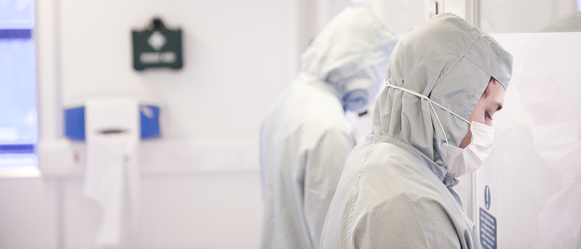
James Watt Nanofabrication Centre
Constructed in 2005, the James Watt Nanofabrication Centre is "a special place", says its director, Professor Iain Thayne. "If you had £100 million to spend, you could go out and buy shiny new versions of all the equipment we have here. But it wouldn't give you capability. You'd be lacking the skills needed to use it. That takes more than just money. It takes expertise and experience which we have built up over almost 40 years."
The foundations were laid in 1978, when University of Glasgow researchers created their own electron lithography tool – the fundamental piece of equipment for nanofabrication - by adapting a scanning electron microscope. The first commercial electron beam lithography tool in any UK university was bought in 1990. The JWNC was built in 2005 to house all the University's micro- and nanofabrication facilities.
"We have grown organically over the decades," says Professor Thayne. "Post-docs and PhD students come and go, but what lasts is the technical expertise. We have 25 technical staff at JWNC, with over 500 person-years of experience."
"In my previous post as a research scientist in a large industrial company, I was having to maintain equipment. If pumps failed I fixed them. If tools broke we worked with the manufacturer to get them operational again. Our post-doc and PhD researchers do none of that. They need to be able to walk in and use equipment that's running to spec and will deliver what they need. It's our technicians that make that happen."
In terms of equipment, the toolset at JWNC is more complete and diverse than in any other UK laboratory, says Professor Thayne. "We have the highest throughput on our e-beam system probably on the planet. Last year we ran for 6,500 hours and completed 3,800 jobs."
Primarily a research facility, JWNC also provides commercial access to industry and governments, through its not-for-profit Kelvin Nanotechnology Ltd. "We delivered 600 wafers last year, for example, for the lasers that fire the information around data centres," says Professor Thayne. "That represented 5% of the global supply, which is impressive for an academic research centre."
Extensive capability
The international standing of the Centre is demonstrated by delivering technology to over 300 companies in 28 countries in the last 5 years (including 12 of the top 20 semiconductor manufacturers) and working with over 90 universities globally.
In terms of research, the diversity of the JWNC toolset supports extensive collaboration. "Significant numbers of research groups around the UK get their nanofabrication from JWNC," says Professor Thayne. "We work on a very diverse range of materials, because we have specific tools for the different chemistries needed to etch those materials and produce devices from them."
Using electron lithography, a pattern can be drawn on the resist over almost any material, as long as it's reasonably flat, says Professor Thayne. "But to transfer that pattern to the substrate the tools needed are material-specific."
Often that material is silicon, the traditional semiconductor, but researchers are now testing a variety of other materials for a wide range of futuristic applications. "They might be dielectrics, for instance, or glasses or compound semiconductor materials," says Professor Thayne. "Being able to support that range of materials makes JWNC very attractive to researchers."
Gallium nitride is an important modern material, for example, with interesting applications. "It can switch rapidly and withstand high voltages, so power electronics is an important application area," says Professor Thayne. "Gallium nitride devices are now being developed to control the motors in electric cars, with the aim of getting the weight down and the mileage up. Another application a little further in the future is wireless power - gallium nitride is an excellent candidate material for that. Then there's augmented reality and acquiring the information on a landscape for use in driverless cars. At JWNC we are working on devices for all these applications and many more."
Besides etching, the other main method of transferring patterns to a substrate is metal deposition. Here too, JWNC supports a broad range of metals and capabilities for a wide variety of applications, says Professor Thayne. "In biomedical devices, for example, you have to be very selective about the materials you use. That's obviously important for lab-on-a-chip, where the device goes into your body. A more recent development is texturing surfaces to control how stem cells express themselves – whether as bone or other tissue, depending on how the surface looks at the nanoscale."
Electron lithography, etching and metal deposition represent three pillars of the sophisticated JWNC edifice. "The fourth is metrology," says Professor Thayne. "It is vital to be able to study and measure everything that we're producing. We use optical microscopes, scanning electron microscopes, surface profilers.
"Our latest tool is a unique system that combines etching capability with a machine that gives chemical and compositional information from the top few nanometres of a surface. Many devices these days are so small that all the interesting stuff happens in that surface layer. So the interaction between it and the underlying material is vital to the properties and quality of the electronic devices you're producing."
Technical expertise and equipment capability, built up over decades, in electron lithography, etching, metallisation and metrology, are what make JWNC so special, says Professor Thayne. "It's the combination of those four technologies - and the diversity of capability we have in each of them - that commends the James Watt Nanofabrication Centre to such a broad and diverse community of users."
JWNC processes at a glance
The James Watt Nanotechnology Centre creates devices with internal structures measured in nanometres, using a variety of materials, for a broad and growing range of applications. These include healthcare, energy, security, nanotechnology, sensors, electronics and quantum technology.
The four technology pillars that support the JWNC are electron beam lithography, etching, metal deposition and metrology.
Electron beam lithography
In electron beam lithography a focused beam of electrons draws patterns on a material called a resist, which is a thin film, spin-coated on the surface of a substrate, usually a semiconductor. Traditionally this would be silicon, but the substrate at JWNC can also be one of a wide range of novel and experimental materials. By altering the solubility of the resist, the electron beam enables selective removal of the exposed regions, the resulting pattern then being used as a mask to create nanoscale structures by etching of, or metal deposition on, the substrate.
Etching
A wide variety of chemical and physical processes at JWNC are used to etch the patterns created by the e-beam into the substrate. The broad division is between wet etching, which uses liquid chemicals, and dry etching, in which chemical gases or high-energy plasmas (similar to sandblasting) remove substrate material. "We have the most diverse set of etching capability in the UK," says Professor Thayne.
Metal deposition
These processes build structures and connections by addition of metal, rather than removal of substrate. Metals used at JWNC include gold, platinum, nickel, aluminium, germanium and titanium. "We spend £70,000 a year on gold alone," says Professor Thayne.
Metrology
Research and quality control at the nanoscale require high resolution optical and atomic force microscopy, combined with detailed chemical and compositional analysis of structures and surfaces.