-Early Stage Researchers (ESR)
ESR 1 Michele Cito
Michele Cito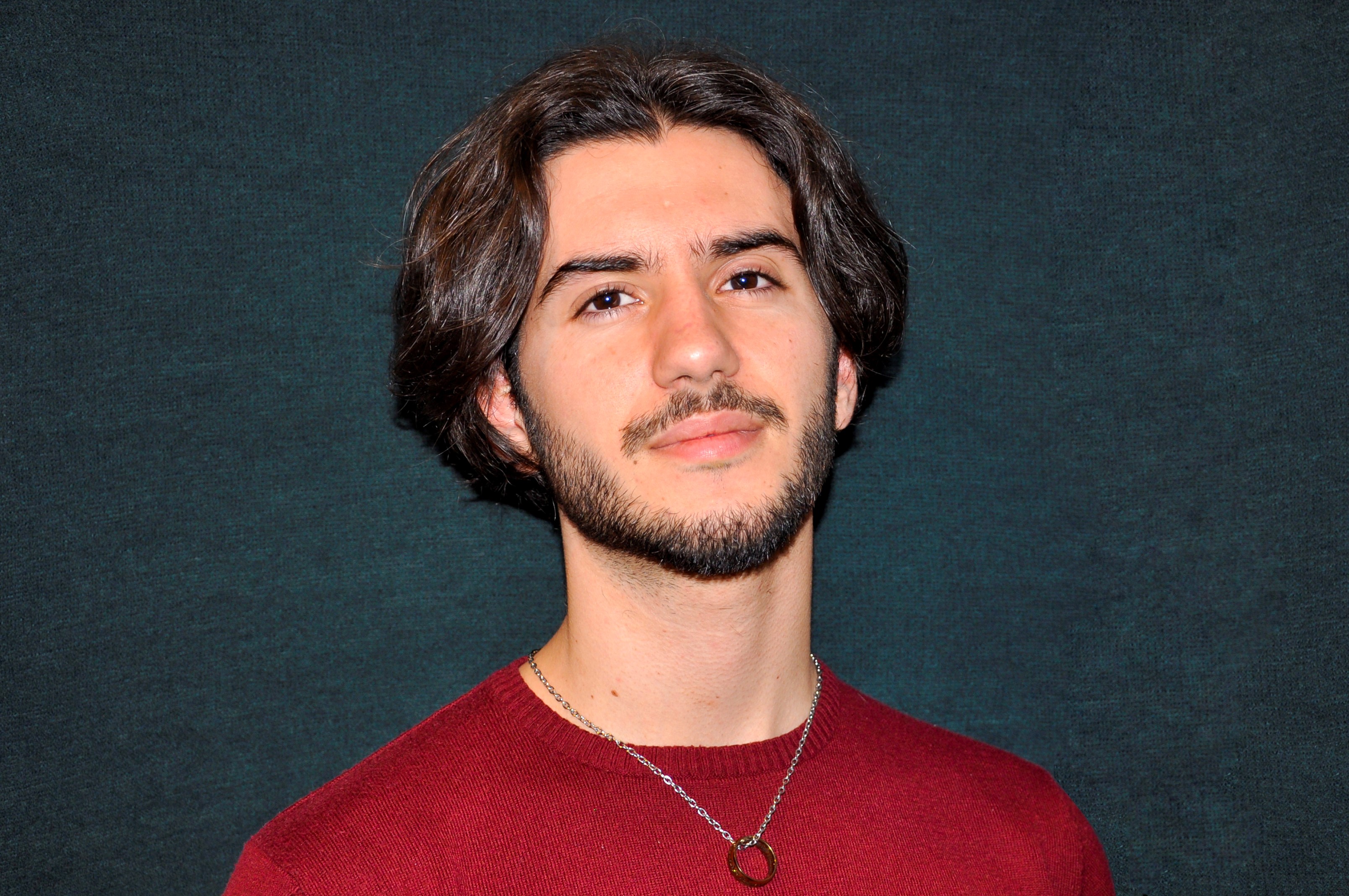
Michele Cito received the Bachelor degree in Electronic and Telecommunication in 2016 and the Master Degree (cum Laude) in Electronics in 2018 from Politecnico di Bari.
During the second year of the Master he collaborates with the Optoelectronics Lab. of Politecnico di Bari lead By Prof. Caterina Ciminelli when he learns about Modelling and simulation of micro, nano and optoelectronic devices.
He also collaborates with Politecnico di Bari as a member of the academic senate and as a tutor for students with disabilities.
He spent 4 months at York University for his master thesis under the supervision of prof. Thomas Krauss, working on an Optoelectronic device in SOI tech. for the study of bacteria Biofilm evolution.
He expanded his knowledge of electronic devices experiencing fabrication and characterization techniques in the clean room.
His research interests cover the field of electronic devices with emphasis for the Biomedical applications.
He is currently working towards the Ph.D. degree in Electrical and Electronic Engineering at the photonics devices group, University of Glasgow(UK), under the supervision of Prof. Richard Hogg (Head of Electronics & Nanoscale Engineering).
As a member of TeraApps Program, he works at the Resonant Tunnelling Diode: Epitaxial Wafer Design, Manufacture and Characterisation.
Other interest/hobby: Rock and Funk Music, painting, cooking, sports, martial arts, classic English Literature and Oriental culture.
Completely immersed in J.R.R. Tolkien world.
ESR 2 Simone Clochiatti
ESR 2 Simone Clochiatti 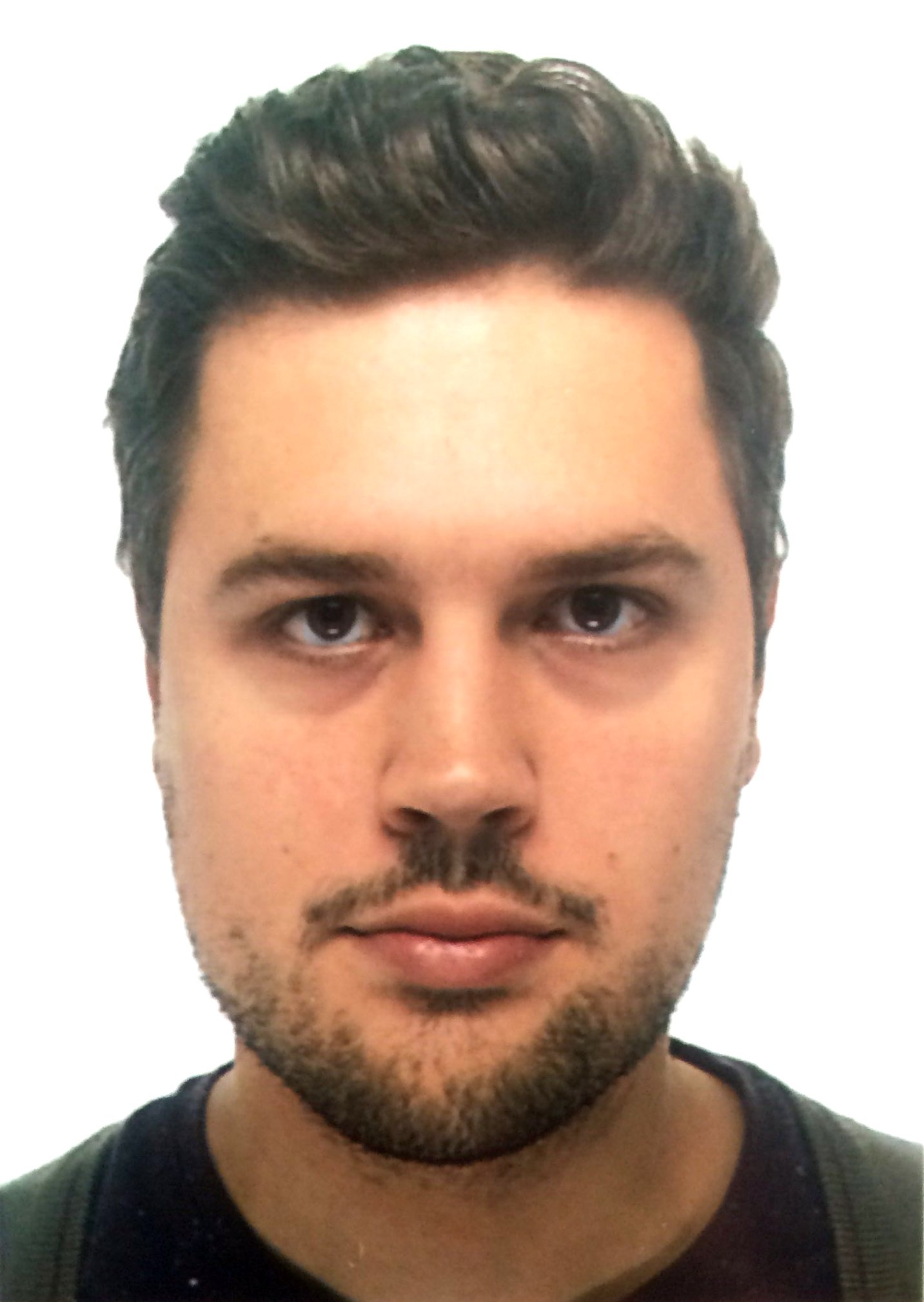
Originally from Italy, completed a M.Sc. in Electrical Engineering at the Technical University of Denmark (DTU), where he followed the 'Wireless Engineering' study line, which provides knowledge in the areas of RF, microwave engineering, and antennas. In a broad sense, these topics were also his research interest and the main motivation that pushed him to move from Italy to Denmark for the Master.
Currently, employed as a Ph.D. student in engineering at the department of components for High-Frequency Electronics at the University of Duisburg-Essen. Within the TeraApps project, he aims to design, characterize and measure integrated circuits for signal generation and detection, based on the Resonant Tunneling Diode (RTD) semiconductor device, operating at the THz frequencies. This circuits will be constituting the power sources needed for THz applications.
ESR 3 Yaksh Rawal
ESR 3 Yaksh Rawal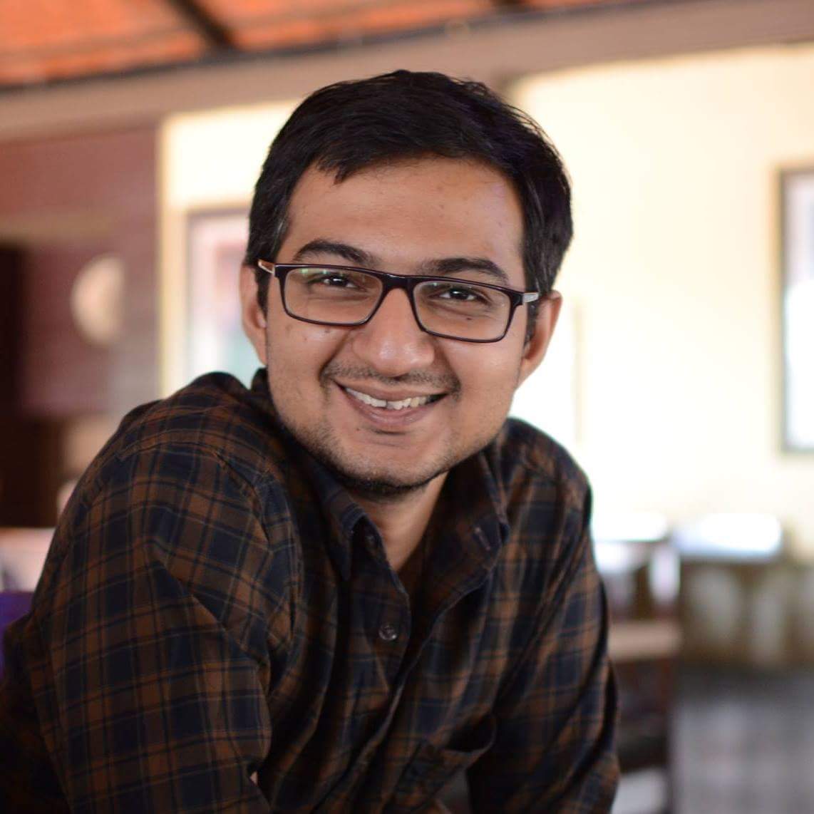
Yaksh is originally from India, where in 2008, he received his Bachelor of Engineering (B.E.) in Electronics from Mumbai University, Mumbai, India. In the year 2010, his interest in microelectronics and semiconductor devices led him to join as project research assistant at Indian Institute of Technology Bombay, Mumbai, India. In 2011, he joined Indian Institute of Technology Bombay as full-time masters student where he worked on fabrication and characterization of metal-insulator-metal tunnel diodes for energy harvesting. After receiving his Master of Technology (M.Tech) in Microelectronics in 2014, he joined again as project research assistant where he worked on contact resistivity reduction for n-Ge source/drain using novel techniques. He has also been teaching assitant at Indian Institute of Technology for courses Solid State Devices, Physics of Transistors, Microelectronics Lab and Electronics Devices and Circuits. During his 5 years(2010-2015) at Indian Institute of Technology, Bombay, he has mentored one graduate student working on MIM capacitors, one intern and one undergraduate student working on Memristor and one undergraduate student working on dielectric constant measurement through capacitance sensing in microuidic channels. In the year 2015-2017, he was employed as Senior Engineer, Integration and Yield, 14nm FinFET group at GlobalFoundries Engineering Private Limited, Bangalore. Working at the forefront of driving yield improvement and product performance during ramp up of advanced technology nodes, 14LPP and 14LPE on GLOBALFOUNDRIES' strategic roadmap. He supported ramp up of these technologies in the new Fab 8 in Malta, NY from GLOBALFOUNDRIES' India centre at Bangalore. He achieved this by monitoring the baseline trends, device parametrics (HOL, FEOL and BEOL) and inline meterology parameters. His main area of focus is on the baseline monitoring and datamining for FEOL parameters.
Currently employed at JMU Wuerzburg as Ph.D student where he'll be working on the design, fabrication (epitaxial growth and nano-structuring) and characterization of resonant tunneling structures in the InAs and antimonide material system on InAs and GaSb-substrates. Electrical transport measurements will be conducted to characterize the electrical performance of the grown resonant tunneling structures as high-speed and MIR optoelectronic devices.
ESR 4 Begum Yavas Aydin
Begum Yavas Aydin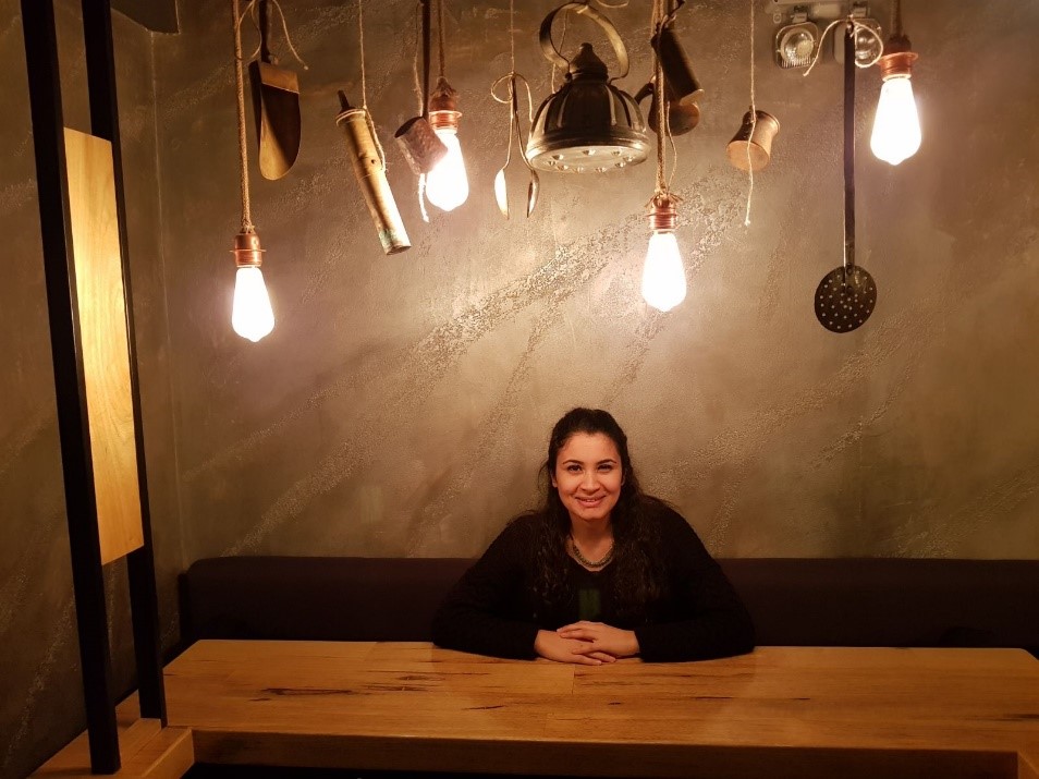
ESR 5 Matteo Villani
Matteo Villani
Matteo Villani got his Master degree in Nanotechnologies for ICTs at Politecnico di Torino, Italy. Its formation is based on deep knowledge of solid state and quantum physics and electronic device theory with a strong direction towards applicability. His final project verted on electrical characterization of Graphene-based nanostructures obtained with self-assembles processes, to verify applicability in switching devices. This research was performed in CEA-LETI laboratories in Grenoble, France.
Within the TeraApps network Matteo has the role of providing simulations support to other partners. Expertise in SSP, quantum physics and photonics are key tools to provide help in analyzing experimental data of other groups in the network.
ESR 6 Davide Cimbri
ESR 6 Davide Cimbri
Davide Cimbri received the B.Sc. in Engineering Physics (Applied Physics) and the M.Sc. in Nanotechnology (both cum laude) from Politecnico di Torino, Torino, Italy. He worked on the M.Sc. thesis at Boston University, Boston, Massachusetts, U.S.A., developing a quantum mechanical-based code to model and simulate the electronic band structure of type-II superlattice mid-infrared (MIR) photodetectors.
He is currently with the High-Frequency Electronics group, division of Electronics and Nanoscale Engineering, University of Glasgow, Glasgow, United Kingdom, working towards the Ph.D. degree in Electronics and Electrical Engineering. His research focuses on resonant tunneling diode (RTD) high-power terahertz (THz) oscillators for communication and imaging applications.
ESR 7 Jehn Zoltan
Jehn Zoltan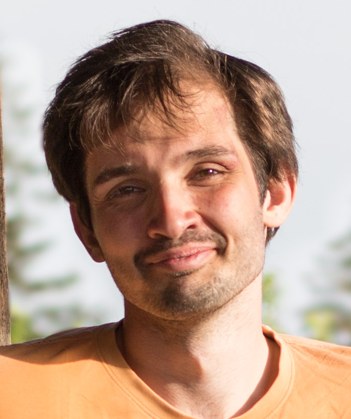
I have done my Bachelor studies at the Technical University of Budapest as physicist, and chemical engineer, and I received my Master diploma at the Technical University of Munich in applied physics. I was involved with the development of the nextnano projects and XienceSim software products. In this project I am mainly interested in the high frequency properties of Semiconductor structures, that can be used for Terahertz radiation. My project is basically a proof of concept of microstrip RTD oscillators, and I am working towards to achieve that. At first on lower frequencies, and then moving to higher frequencies.
In my free time I tend to build anything from wood, and when my schedule allows I watch art movies.
ESR 8 Meng Zhang
Meng Zhang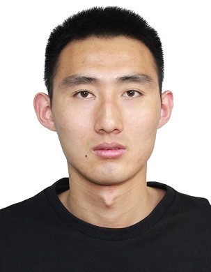
Meng Zhang, come from China. He got his bachelor and master degree from Beijing Institute of Technology at 2015 and 2018, respectively. He majored in Electrical Engineering in bachelor period. In the master period, his research and study areas are mainly in the Millimetre wave and Terahertz technology. He participated in the research topics such as, metamaterial, quasi-optical device, THz on-chip antenna, compact antenna test range and so on.
Currently, he is employed as a Ph.D student in General and Theoretical Electrical Engineering at the University of Duisburg-Essen. In the TeraApps project. He mainly charges for the antenna design for Resonant Tunneling Diode (RTD) semiconductor device that operates at terahertz frequency. In transmitter, the same antenna will be used to achieve the wireless sub-harmonic injection locking to improve the performance the RTD. In receiver part, a broadband high gain on-chip antenna will be designed.
ESR 9 Saif Alomari
Saif Alomari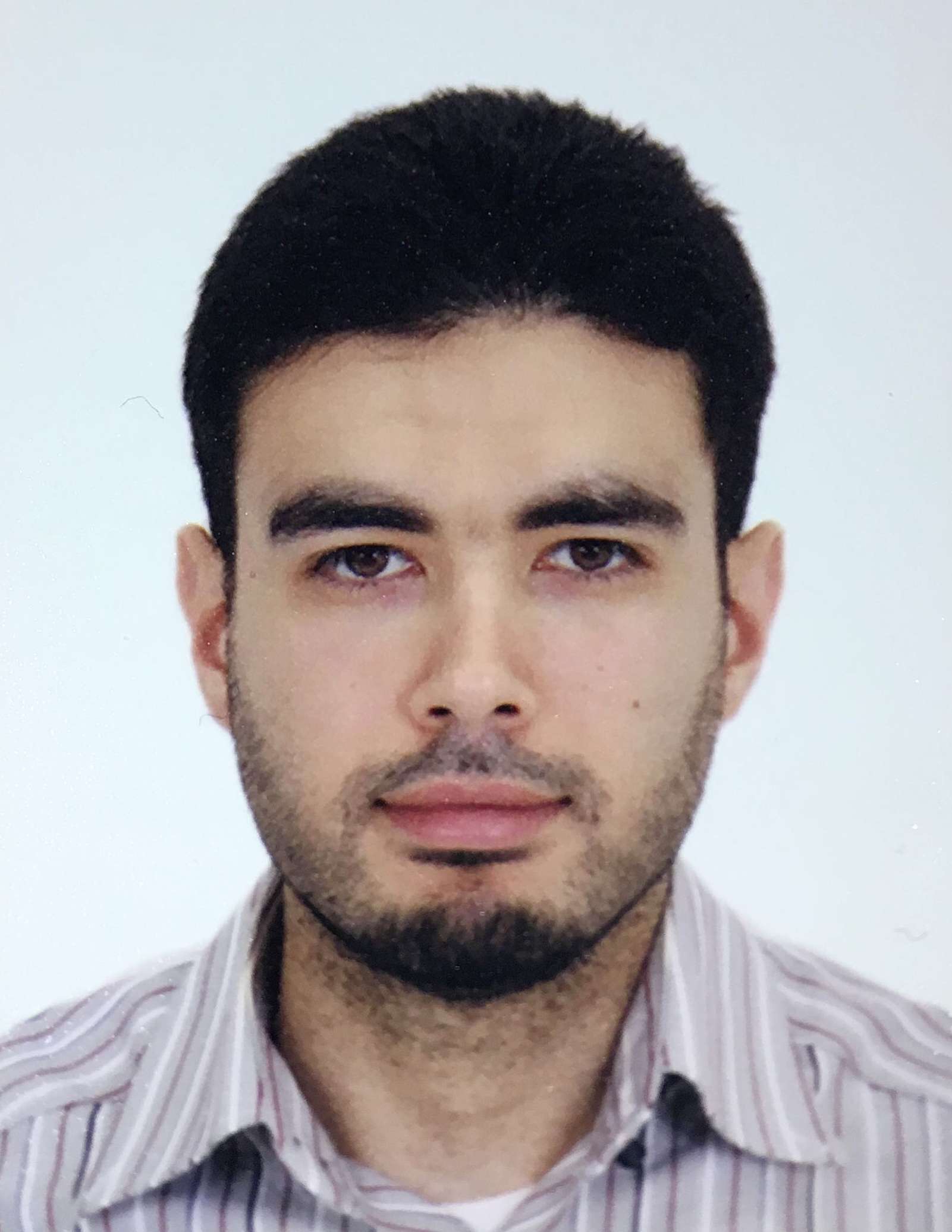
I have a bachelors’ degree in electrical engineering from the university of Jordan, and around 6 years of industry experience. In 2017 I graduated from the university of Leeds with a master’s degree in electronics and electrical engineering. I am extremely interested in novel semiconductor devices, particularly those utilizing quantum mechanical effects and their huge potential use as enabling technologies for next generation circuits and systems. I have worked on the fabrication of resonant tunneling diodes during my master’s project using GaAs wafers. For my PhD I am aiming at deepening my understanding in optoelectronics and hoping to produce opto-electronic circuits based on RTDs and laser diodes that can work as high sensitivity, high speed photo detectors.
In my free time, I like to read books, sketch, and sometimes go on hiking.
ESR 10 Sebastian Gebert
Sebastian Gebert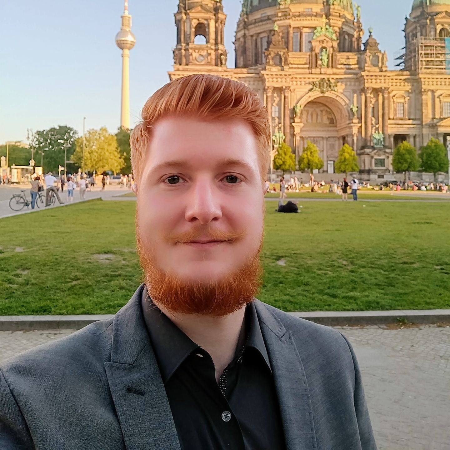
Sebastian Gebert conducted his studies at the University of Regensburg (UR) in Germany. During his bachelor thesis he began working on 2D topological insulators by investigating THz radiation induced photocurrents. Subsequently, he worked as a student assistant focusing on photogalvanic spectroscopy of (Bi,Sb)Te based 3D topological insulators. He is currently finishing his Master of Science (Physics) dedicated to nonlinear photocurrents and photoconductivity induced by intense THz radiation in HgTe-based quantum well structures and will participate the TeraApps project at Montpellier later this year. His focus will be the investigation of new 2D materials for Imaging and telecommunication applications.
ESR 11 Mahdi Asgari
Mahdi Asgari
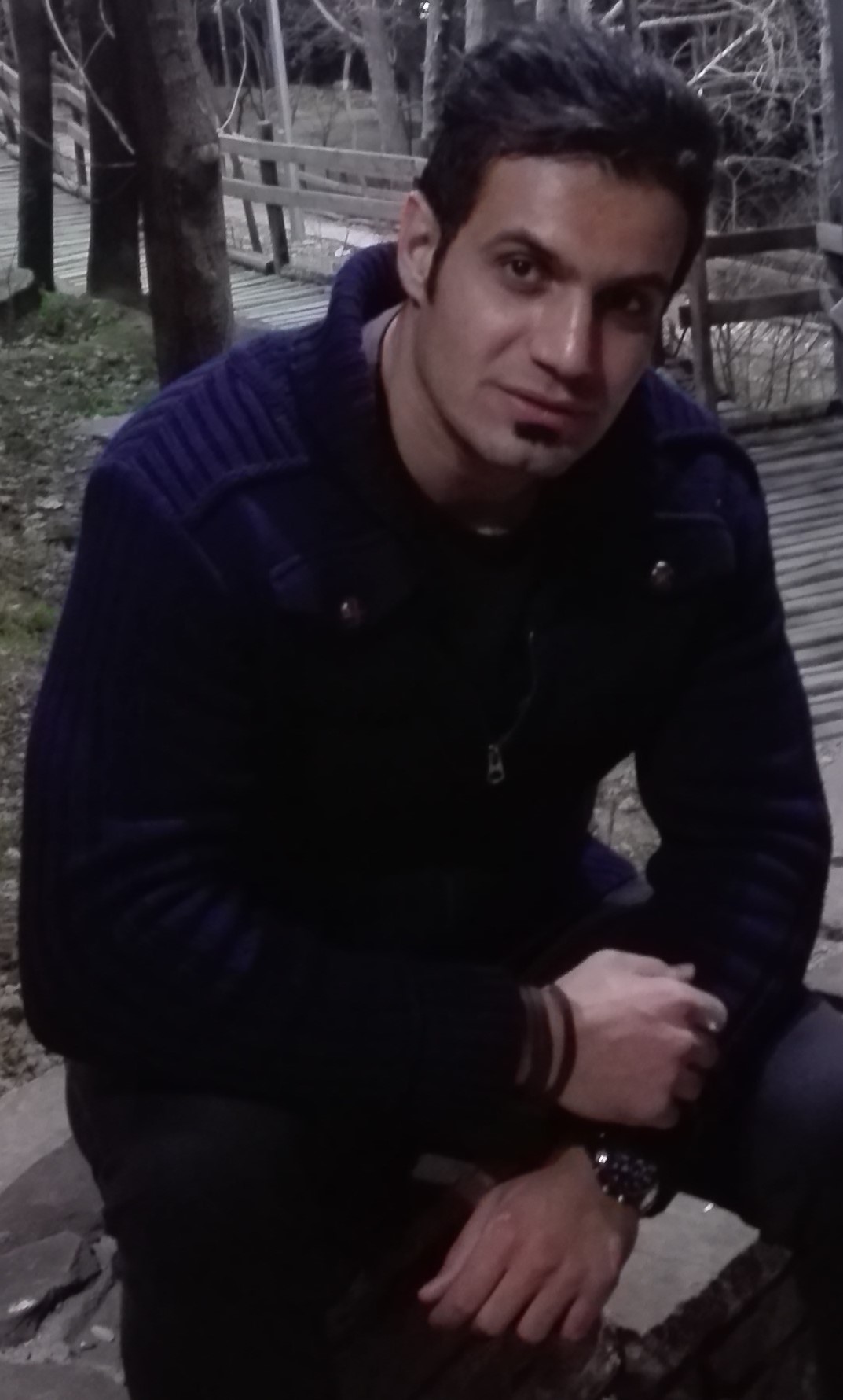
This project has received funding from the European Union’s Horizon 2020 research and innovationprogramme under the Marie Skłodowska-Curie grant agreement No 765426”. Originally from Iran where I acquired my bachelor degree in Atomic and Molecular Physics from Kharazmi University in the year 2013. Afterward, I went to K.N.Toosi University of Technology where I got graduated from in 2016 so that my research areas in connection with MSc. degree thesis include, but are not limited to, condensed matter physics, many body particle physics and, most importantly, unconventional superconductors. However, my research were extended to other interdisciplinary projects, particularly medical physics in which I have been working on laser therapy in combination with gold nanoparticles for cancer treatment through simulation utilizing Monte Carlo and Finite Element Methods as well.
Nowadays I am working in Italy as a PhD student of Scuola Normale Superiore University at National Enterprise for nanoScience and nanotechnology (NEST) upon not only fabrication, but also characterization and development of room-temperature high speed THz photodetectors based semiconductor nanowires field effect transistors as well as THz plasmonic and thermoelectric detectors based new layered materials. Furthermore, I aim to couple QCL frequency with s-SNOM to exploit Near-Field scanning optical microscopy in my current project.
Meantime, whenever I can find free time, I would prefer to get involved in sport specifically gym.
ESR 12 Thomas Nowack
Thomas Nowack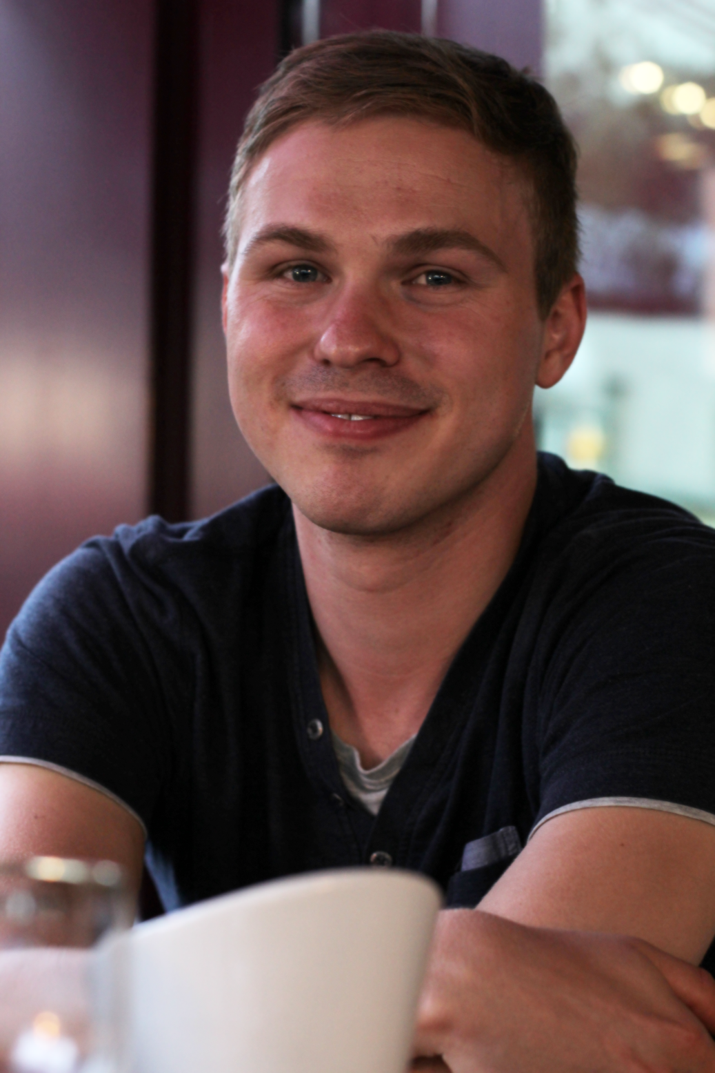
For his Bachelor’s, Thomas studied Functional Materials Technology at the Julius- Maximilians-Universität Würzburg, which provided him with a broad scientific background ranging from chemistry & analytic methods over electronics & engineering to physics & nanotechnology, with focus on materials science. Aiming at applied science, all topics were taught with significant stress on tailoring materials towards their targeted applications under consideration of their technological feasibility. Towards the end of his Bachelor, the field of organic electronics caught his interest due to its interdisciplinary approach to engineer (opto-) electronic devices employing chemistry, physics and molecular (nano-) engineering.
He consequently joined the international Master’s program Organic and Molecular Electronics at the Technische Universität Dresden. The program deepened background and interest in Micro-/Nanotechnology, electronics, semiconductor technology, molecular physics and especially in optoelectronics. For his Master’s Thesis, he joined IMEC as international scholar of the Katholieke Universiteit Leuven to work on the process-integration of organic thin-film transistors by photolithographic patterning.
He is consequently especially interested in the tailored development of advanced materials and their integration into functional optoelectronic devices.
Within the TeraApps project, he aspires to develop ultra-compact, highly efficient metamaterial-based optics for imaging in the Terahertz range. The produced meta-optics is hereby i) easily integrated into compact imaging systems with novel low-power sources developed within TeraApps, as well as ii) enabling novel functional imaging, providing extended information on the sample (e.g. 3D-imaging, Dichroic imaging, etc.). Expected scientific output is hence the demonstration of a prototye THz imaging system.
ESR 15 Robin Schmidt
Robin Schmidt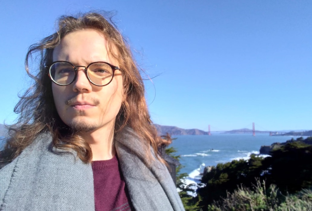
Originally from France, Robin graduated in 2018 as an Electrical Engineer from l'Ecole Superieur d'Electricite and got his master's degree from Paris Sud university the same year. Moved by his profound interest in applied physics, he has been searching to marry this passion with electronic design, which led him fast towards high frequency electronics.
Introduced to Terahertz technologies within Paris Sud, his interests for the domain grew since there is still a lot of fundamental research to follow in that domain, particularly for metrology, which demand a strong physic background, programming skills, and statistical modeling.
Now employed as an Early Stage Researcher by Keysight Technology Belgium, his focus will be the development of metrology level calibration structures for on wafer S-parameters measurements in mm and sub-mm-wave frequency. A comprehensive study on uncertainties pending in those measurements will be followed.
Within the TeraApps network, he will provide the knowledge to choose for the best measurement strategy for any relevant devices designed.
Sharing good moments, nature and music are his main resources.


