

Scientists develop world’s smallest diamond transistor
Published: 9 April 2009
Scientists in the Department of Electronics & Electrical Engineering have developed the world’s smallest diamond transistor.
Scientists at the University of Glasgow have developed the world’s smallest diamond transistor.
At just 50 nanometres in length the ‘gate’ of the diamond transistor developed by Dr David Moran, of the Department of Electronics & Electrical Engineering, is more than 1000 times smaller than the thickness of a human hair, and is half the size of the previous smallest diamond transistor developed by Japanese firm NTT.
Diamond is heralded as being an ideal material for the next generation of nanoscale electronic devices due to its amazing and unique properties and could help scientists develop nascent technologies such as Terahertz Imaging and Automotive Collision Detection.
The ‘gate’ of a transistor is used to control the flow of current between two electrical contact points, acting as a switch or an amplifier. The smaller the gate, the faster the transistor works.
Dr Moran said: “From its invention in 1947, the transistor has been the building block of many modern day technologies, from silicon based chips in your computer processor, to gallium arsenide based circuits in your mobile phone.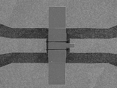
“These types of materials – silicon and gallium arsenide – are chosen upon what their strengths and weaknesses are. Diamond on the other hand is very much an excellent all-round performer, and has been described by many as a perfect material.
“By developing a diamond transistor technology, we aim to tap into the truly amazing properties of this exciting material which could prove fundamental to the development of several next generation technologies.”
Such technologies include Terahertz Imaging and Automotive Collision Detection.
Terahertz imaging uses terahertz radiation (T-rays) – electromagnetic waves of a frequency range between that of microwaves and infrared which can penetrate a range of materials, including clothes and flesh – to create a picture.
Because it is non-ionising, it does not damage cells and has potential applications in
security scanners to detect concealed weapons through clothes as well as safer medical imaging.
Automotive collision detection or automotive radar is an advanced safety feature currently being heavily researched by the car industry with which a car or other automotive vehicle will have an effective radar zone around it that will allow it to detect potential collisions from any side of the vehicle well in advance and take avoiding action.
Dr Moran added: “These applications require a very fast and ideally high-power transistor technology that needs to be able to operate in adverse weather/temperature conditions. This is where a diamond transistor technology would excel”.
The diamond itself is artificially made by UK firm Element 6 through a process called chemical vapour deposition.
The creation of the tiny device is part of a five-year project funded by the Engineering & Physical Sciences Research Council (EPSRC) and is the result of a collaborative project between the University of Glasgow and Heriot Watt University. Its construction was only possible through the multi-million pound facilities within the James Watt Nanofabrication Centre at the University of Glasgow where electron beam lithography was employed to create patterns and structures on the miniscule sliver of diamond.
The University of Glasgow has one of the most advanced large area high-resolution electron beam lithography tools in the world.
For more information contact Stuart Forsyth in the University of Glasgow Media Relations Office on 0141 330 4831 or email s.forsyth@admin.gla.ac.uk
First published: 9 April 2009
<< April