

UofG nanofabrication facility marks 20 years of achievement
Published: 26 March 2026
A Scottish high-tech manufacturing facility which helped create the technology that runs the modern internet is celebrating its 20th anniversary.
A Scottish high-tech manufacturing facility which helped create the technology that runs the modern internet is celebrating its 20th anniversary.
The University of Glasgow’s James Watt Nanofabrication Centre is one of the UK’s key facilities for research, development and training in nanoscale devices.
The facility is home to a £35m suite of equipment which enables a wide range of cutting-edge applications and has supported the work of nearly 200 high-tech companies around the world.
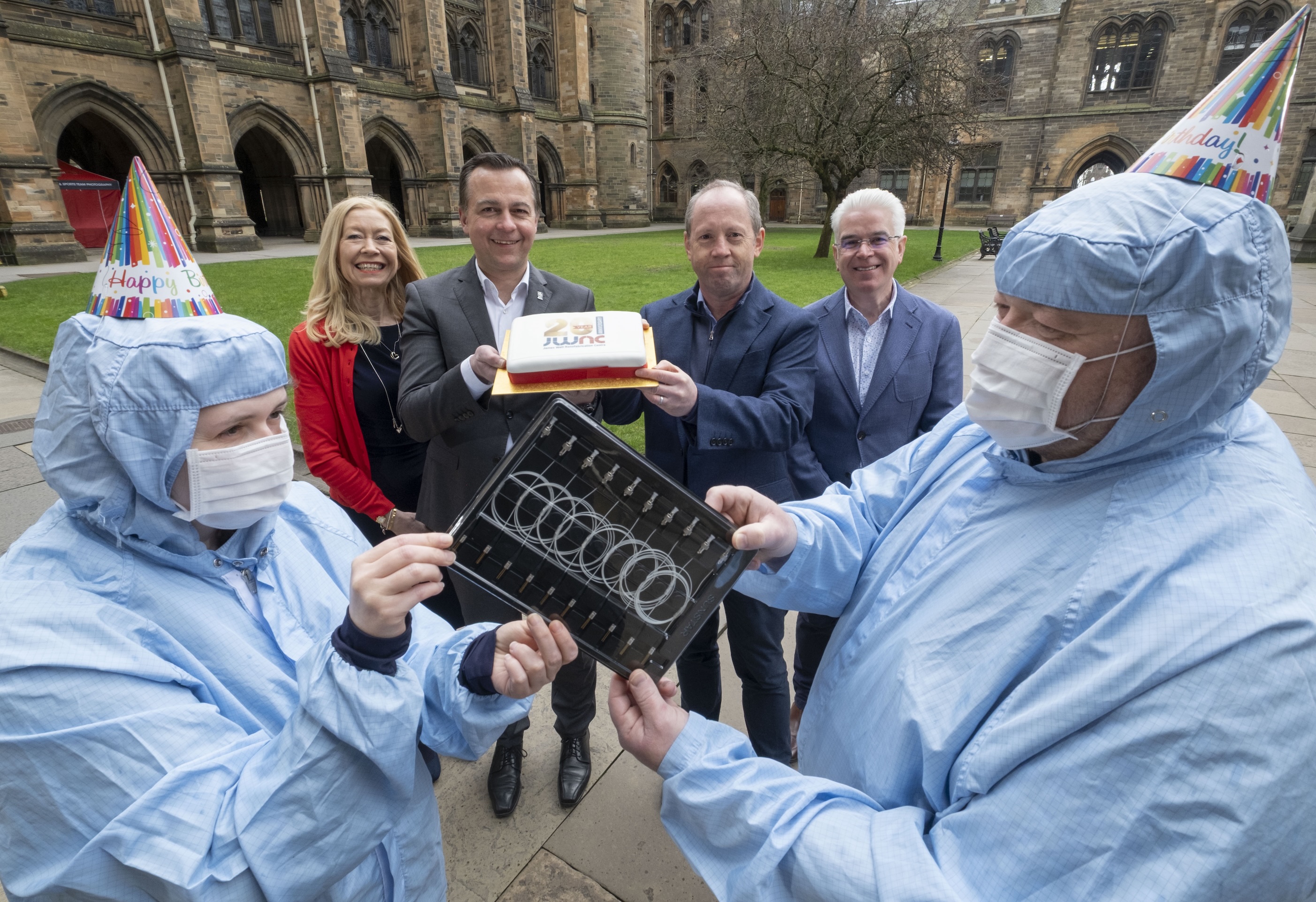
(centre l-r) JWNC director of strategy Evelyn Toma, JWNC director Professor Martin Weides, Sivers Semiconductor CTO Andrew McKee and Kelvin Nanotechnology CEO Brendan Casey are flanked by JWNC staff in cleanroom suits holding laser components developed by Sivers and manufactured in partnership with the JWNC. The JWNC staff are Claire Goodwin (left) and Mark Dragsnes (right).
Since the facility’s first test run on 26th March 2006, JWNC researchers have established a string of world records, witnessed their groundbreaking technology used to see far below the Earth and on board the International Space Station, and trained hundreds of postgraduate students who now contribute to the world’s tech giants.
It has also helped establish a series of spinouts which are commercialising fundamental research in sectors including healthcare, quantum technologies and photonics, and it plays a key role in supporting Scotland’s thriving critical technologies sector.
However, it’s the Centre’s work on fabricating custom semiconductor lasers used in the world’s largest data centres which has had the most impact over the last two decades.
In 2016, Sivers Semiconductors won volume production contracts to supply lasers for fibre-optic communications thanks to the support and expertise of the JWNC. These products enabled faster optical fibre internet and television services to consumers, shipping on a global scale.
Working closely with the University’s commercial subsidiary Kelvin Nanotechnology (KNT), the JWNC helped Sivers produce millions of lasers to deploy in optical network applications around the world, using the Centre’s electron-beam lithography tools. The tools use a focused beam of electrons to etch intricate patterns just a fraction of a micron across, enabling the creation of tiny photonic devices.
Andrew McKee, Sivers Semiconductors’ CTO, said: “Based on the early development work done at the JWNC, Sivers has today supplied 45 million advanced lasers into a wide range of applications including AI datacentres, LIDAR and consumer sensing. That’s a remarkable achievement for a Scottish company, and part of the credit for that belongs to the JWNC.
“Working with KNT and the JWNC gave us rapid access to world‑leading equipment and expertise which accelerated our time to market by around 18 months. That speed was crucial in winning business and establishing us as a global technology leader, and becoming a key strategic supplier to many Fortune 100 and Silicon Valley start-up customers that we are today.”
The early commercial success enabled Sivers to scale quickly, build a world‑class internal team and diversify its portfolio. The company is now one of the world’s leading suppliers of lasers that enable high‑speed optical interconnects for AI processing.
As Scotland’s leading electron‑beam lithography facility, the JWNC now conducts more than 100 e‑beam jobs each week, supporting a University research portfolio worth more than £53 million. Its 1,200‑square‑metre cleanroom hosts tools enabling the creation of advanced electronic, optoelectronic and bio‑compatible devices. Today the Centre employs 26 full‑time staff, with a further 20 working at KNT.
Professor Martin Weides, director of the James Watt Nanofabrication Centre, said: “The University of Glasgow has been at the cutting edge of nanofabrication over six decades, from establishing our first e-beam in 1978 by converting a scanning electron microscope, to buying the UK’s first commercial e-beam tool in 1990, to our leading position today.
“However, it was the first electron fired from our e-beam tool by Dr Stephen Thoms on Sunday 26th March 2006 that sparked a remarkable expansion of the University’s capabilities which has surpassed even our initial ambitions. The Centre has more than doubled in size over its lifetime, helping us play a leading role in advancing fundamental research, enabling commercial partnerships, and supporting global and domestic supply chains.
“Over the course of the last 20 years, the JWNC’s facilities and our uniquely talented staff have helped take research out of the lab and into commercial use. We have helped fabricate prototype parts for major international companies to use in everyday devices like mobile phones, as well as established our own spinouts across sectors of industry which will help spur economic growth.”
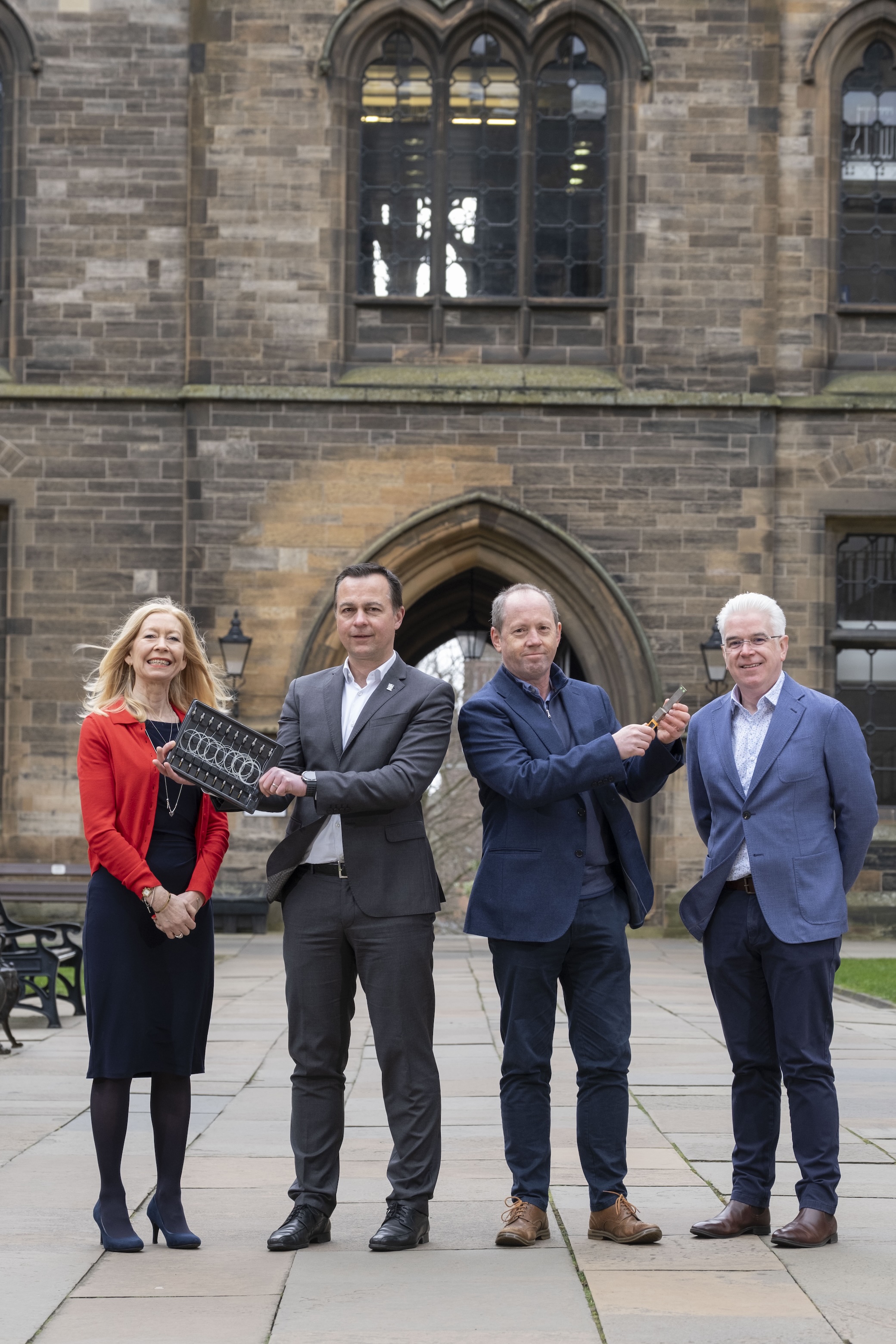
(l-r) JWNC director of strategy Evelyn Toma, JWNC director Professor Martin Weides, Sivers Semiconductor CTO Andrew McKee and Kelvin Nanotechnology CEO Brendan Casey hold components developed by Sivers and manufactured in partnership with the JWNC.
Kelvin Nanotechnology has supported more than 170 companies across 23 countries, while University researchers have launched multiple spinouts including Vector Photonics, Neuranics, and Gold Standard Simulations.
Over the last two decades, JWNC’s facilities have supported breakthroughs including the smallest e‑beam lithography pattern at three nanometres, the best layer‑to‑layer alignment at 0.46 nanometres, and the world’s smallest diamond transistor. Techniques developed at the Centre enabled the creation of the world’s fastest diamond transistor in 2009 and the world’s smallest diamond coin in 2012. Devices fabricated at the JWNC have been used to monitor volcanic activity on Mount Etna, measure air quality on the International Space Station, and develop quantum cascade lasers for applications ranging from explosives detection to defence countermeasures.
Each year, more than 200 postgraduate students train in the Centre, with alumni now working across the global tech ecosystem at companies including Google, Microsoft, ASML, Micron and BAE Systems.
Now, the Centre’s leaders are setting their sights on establishing an even more ambitious facility in the years ahead. A proposal for a new facility, called the Critical Technologies Nanofabrication Facility (CTNF), is under development.
The CTNF will aim to take critical technologies from the lab to commercial deployment. The facility will build on the JWNC’s expertise to expand the UK’s capability in rapid prototyping and low volume production for SMEs and corporates, reducing their reliance on offshore manufacturing. It will also train highly-skilled staff and contribute to UK economic growth and national security.
Evelyn Toma, the JWNC’s director of strategy, said: “As proud as we are to be celebrating two decades of achievement, particularly during the University of Glasgow’s own 575th anniversary year, our plans for the next phase are about scale and impact. Our ambition is that the CTNF will help companies take critical technologies from lab to market faster and more securely, while training the people who will build the next generation of devices here in the UK.”
First published: 26 March 2026