

Facilities
 Our suite of instruments provide powerful techniques for investigating materials at lengths from the sub-millimetre right down to the atomic scale. These instruments are world-leading in many of their capabilities and our research staff have developed many unique imaging modalities.
For more information on the capabilities and specifications of our instrumentation please visit the links below:
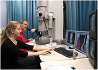
Transmission Electron Microscopes (TEMs)
We operate two unique and highly advanced TEMs that enable the imaging and analysis of materials with resolution from nanometre to atomic scale. Example applications are investigating the structure of bulk materials including defects, voids, cracks; interface quality and levels of strain in thin films and layered materials.
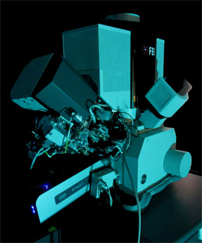
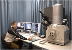
 JEOL ARM200cF - "MagTEM"
This world-leading electron microscope can scrutinise individual atoms and probe their chemical, magnetic and electronic properties with unprecedented detail.
It can resolve a much greater level of detail than we have been able to in the past and offers invaluable support for the next generation of technology development. In studies of the types of magnetic materials commonly found in computer hard disk drives we are able to see magnetic details in materials around 10 times smaller and examine nanoscale events occurring in spans of time more than one million times faster than before.
In combination with a Gatan GIF Quantum electron spectrometer, the MagTEM microscope can help commercial partners develop and refine technologies including stronger forms of steel for the automotive industry, sensor systems and hard disks. MagTEM’s magnetic imaging capabilities will allow it to image the operation of magnetic devices such as hard disks below the dimensions of individual storage bits, a process which no other electron microscope in the world is currently capable of doing.
Specifications
Imaging
- Accelerating Voltage from 200 kV down to 60 kV for low-damage imaging.
- Electron Source: cold field emission gun for high brightness, high resolution study.
- Beam energy spread (FWHM) down to 0.27 eV for high resolution spectroscopic analysis.
- Aberration correction (probe) to achieve sub-atomic spatial resolution, down to 0.078 nm
- Tomography capability for three-dimensional visualisation
- Variety of sample rods, offering the capability for analysis between 100 K and 450 K, in-situ electrical connections, high-tilt (tomography) imaging, low background x-ray analysis, etc.
- Gatan Orius camera for TEM image acquisition, scanning diffraction, etc.
- Variety of STEM detectors including the capability for annular bright-field imaging for direct visualisation of light elements.
- Removable Medipix3 direct electron detector (256x256 pixels) with Merlin readout capable of > 1000 fps and control for use as a STEM detector synchronised with the scan.
- Nanomegas system for precession electron diffraction using the Merlin for electron counting based readout (electron shot noise only)
Chemical mapping
- Gatan 965 Quantum ER spectrometer with high-speed option for fast, wide-area microanalysis. The spectrometer includes 'DualEELS' functionality that was originally developed in collaboration with the University of Glasgow.
- EELS spectrum acquisition at up to 1000 spectra/second
- Zero-loss filtering of images and diffraction patterns
- Bruker XFlash (60mm2) EDS detector for x-ray mapping.
Magnetic and Electric field imaging
- Full hardware and software functionality for Lorentz imaging of magnetic media
- Customised control and reversal of magnetic field conditions around the sample for zero field analysis and hysteresis measurements.
- World-leading, sub-nanometre, aberration-corrected spatial resolution with zero field at the specimen, derived from collaboration with JEOL.
- Custom, 8-segment detector for quantitative differential phase contrast imaging.
- Differential phase contrast imaging with the Merlin/Medipix detector (centre-of-mass and edge detection).
In-situ TEM capabilities
- DENS Solutions combined heating & biasing holder.
- Gatan heating holder.
- Gatan cryogenic liquid nitrogen holder.
 FEI Tecnai T20
- Conventional imaging
- Elemental mapping
- Crystallographic diffraction analysis
This transmission electron microscope is equipped with a Gatan image filter, which allows the energy filtering of images, so that for instance images can be quickly generated for a specific energy loss allowing the relatively fast generation of elemental maps. This can also be used to filter all energy loss electrons from an image just leaving the zero-loss electrons, which results in a reduction of the diffuse scattering contribution and thus a sharper image.
This microscope will have wide applicability for both micro- and nano-structural studies of materials, as well as elemental mapping using the Gatan image filter.
Specifications
Accelerating Voltage: 200 kV
Electron Source: LaB6 filament
Objective Lens: FEI Supertwin
- Cs = 1.2 mm
- Point resolution = 2.4
- Line resolution = 1.5
- Atomic resolution possible in many materials
- Allowable goniometer tilt about 40 / 30 (double tilt)
Alternative Lorentz objective lens for magnetic studies
- Objective lens current can be reverse for magnetisation studies
Gatan Image Filter, GIF 2000
- CCD Camera for image acquisition
- Elemental mapping via energy filtered imaging
- Zero-loss filtering of images and diffraction patterns
- Using the microscope's "EFTEM" lens programme can achieve magnifications from < 10 kx to > 1000 kx
- Suitable for all kinds of image from low-magnification microstructural imaging to high-resolution imaging of atomic columns
SIS Megaview III CCD camera
- High acquisition rate imaging of images and diffraction patterns
- Can be controlled from within TIA
- Mounted at the 35mm camera port providing a wide field of view ideal for low magnification imaging or imaging of low camera length diffraction patterns
Gatan off-axis TV-rate camera
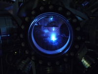
Xenon Plasma Focused Ion Beam Microscope
Helios Plasma Focused Ion Beam (PFIB) for Materials Science
The microscope is equipped with the following:
- Xenon plasma ion beam column
- FEG-SEM column at 52 to the ion column
- In-lens detector with secondary and backscatter modes
- Secondary electron detector
- ICE detector (for ion imaging)
- Directional backscatter detector
- Integrated plasma cleaner
- Multichem gas injection system with Carbon and Platinum precursors
- Separate cobalt and iron precursor gas injector systems
- FEI Easylift NanoManipulator
- Bruker XFlash 100 mm2 EDX detector
- Bruker eFlash FS EBSD detector
- Bruker Esprite QUBE 3D reconstruction and data handling software.
Please contact phas-knc@glasgow.ac.uk if you wish to gain access to this machine for academic or industrial projects.
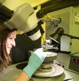
Focused Ion Beam / Scanning Electron Microscope (FIB-SEM)
Our dual column FIB-SEM instrument is a versatile tool that enables sub-surface and 3D investigation of materials, precise extraction of ultrathin TEM sections and nano-patterning.
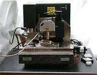
 DualBeam Focused Ion Beam (FIB) System
- Preparation of transmission electron microscope specimens from specific sample regions
- Local property modification by irradiation to produce patterbed magnetic films
- Definition of magnetic or other nanostructures
- Reconstruction of 3D sample structures through serial sectioning techniques.
The microscope is equipped with the following:
- Sidewinder ion column
- FEG-SEM column at 52 to the ion column
- Omniprobe 100 micromanipulator
- Platinum and tungsten deposition facilities
- Oxford Instruments INCA Energy Dispersive X-ray analyser
The Sidewinder column gives a well defined ion probe shape at large probe currents, allowing more accurate rapid removal of material, and also the ability to form small ion probes down to 2 keV energy, allowing excellent final polishing to remove surface damage.
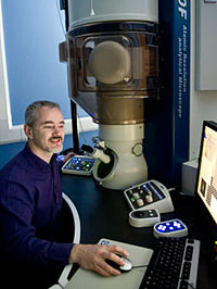
Atomic Force Microscopes (AFMs)
AFMs provide multiple imaging modes for measuring the properties of surfaces. These include mapping of surface height (topography), resistivity, mechanical properties, ferroelectric domains and P-E hysteresis and magnetic domains.
 Veeco Dimension 3100 Scanning Probe Microscope
This microscope provides rapid assessment of surface topology, roughness, and structure as well as the magnetic and electric properties of a sample.
Specifications
- Contact and non-contact mode atomic force microscopy with sub-nanometre vertical resolution
- Electric force microscopy capability
- Magnetic force microscopy capability
- Custom in-situ magnetisation stage
- Automated sample positioning and large-area scanning platform: inspectable area size = 1200 mm x 100 mm
- Holds up to 8" diameter samples
- Sample scanning under ambient, atmospheric conditions
- Video image capture capability
- Dedicated PC and analysis software
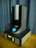 NT-MDT Solver NEXT
This scanning probe microscope offers a vast range of techniques for surface and electrical characterisation of materials down to nanometric lenghtscales.
Specifications
- Contact, non-contact and tapping mode atomic force microscopy with sub-nanometre vertical resolution
- Industry-leading automation level
- Lateral force microscopy
- Electrostatic force microscopy
- Magnetic force microscopy
- Scanning Kelvin probe microscopy
- Piezoresponse force microscopy
- Nanolithography
- Spreading resistance imaging
- Atomic force spectroscopy
- Video image capture
- Dedicated PC and data processing software
Neocera Pulsed Laser Deposition (PLD) system
 We have access to a variety of sample fabrication and thin-film deposition systems for deposition and patterning of thin films. In particular, a pulsed laser deposition system has recently been installed for the deposition of oxides and alloys, incorporating a RHEED system for in-situ analysis and controlled deposition at the monolayer level. Other facilities are dedicated to the deposition of metallic and carbon thin films and coatings. Please contact us for further information.